CCD vs CMOS: Difference Between CCD and CMOS Image Sensor
Jan 24, 2024 View: 1944
CCD and CMOS sensors stand out as the prevailing types of photosensitive sensors in contemporary usage, finding extensive applications in digital cameras, camcorders, camera phones, astrophotography, radiography, and webcams. While both are widely employed, they exhibit distinctions in terms of structure, performance, and technology. This article will delve into the specifics of CCD and CMOS sensors, providing an analysis of their differences.
Catalog:
CCD and CMOS Full Form
What is CCD and CMOS
CCD vs CMOS: Working Diagram
CCD vs CMOS: Main Difference
CCD vs CMOS Sensor: Image Quality
CCD vs CMOS: ISO Sensitivity
CCD vs CMOS: Resolution
CCD vs CMOS: Noise
CCD vs CMOS: Power Consumption
CCD vs CMOS: Cost
CCD vs CMOS: Backup Camera/Reverse Camera
CCD vs CMOS: Color
CCD vs APS-C
CCD vs CMOS: FPV Cameras
CCD vs CMOS: Pros and Cons
Final Words
FAQ
CCD and CMOS Full Form
CCD stands for "Charge-Coupled Device," and CMOS stands for "Complementary Metal-Oxide-Semiconductor." Both are types of image sensors used in digital cameras and other imaging devices.
What is CCD and CMOS
CCD (Charge-Coupled Device) and CMOS (Complementary Metal-Oxide-Semiconductor) are two types of image sensors found in cameras and imaging devices. They differ in their manufacturing processes, with CCD using the LSI manufacturing process, and CMOS based on the CMOS LSI manufacturing process.
In the case of CCD, the pixel charge packets need to be sequentially moved to the shift register, whereas CMOS directly reads the signal of each pixel. CCDs transfer light-generated charge from one pixel to another, converting it into voltage at the output node. On the other hand, CMOS imagers use multiple transistors on each pixel to convert the charge within each pixel into voltage.
CCD and CMOS Sensor Technology
CCD production technology is well-established, employing PN structure or silicon dioxide isolation layers to isolate noise. This maturity contributes to CCD's imaging quality, which holds certain advantages over CMOS. In CCD, each row of pixels shares an "amplifier" for signal processing, while CMOS has a separate amplifier for each pixel. Additionally, the photosensitive area of CCD is generally larger than that of CMOS under the same size because CMOS allocates space for integrating complex circuits. As a result, CCD tends to deliver better image quality compared to CMOS.
CCD (Charge-Coupled Device)
CCD (Charge-Coupled Device) is a detection element that utilizes coupling to transmit signals, serving as a semiconductor component capable of converting optical signals into digital signals.
The structure of CCD includes micro lenses and color filters, distinguishing itself by having photosensitive components on its surface arranged in a matrix with the ability to store charges. When light interacts with the surface, the resulting charge reactions in these components collectively form a complete picture across the entire CCD.
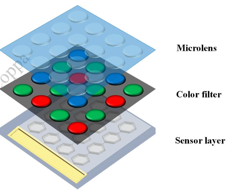
Micro lenses constitute the first layer of the CCD. To enhance the light-gathering efficiency, the light-receiving area of a single pixel needs expansion. However, the method of increasing the light-gathering rate can potentially compromise image quality. Introducing a layer of "micro-lens" functions like adding a pair of glasses, determining the photosensitive area not by the sensor's opening but by the micro lens's surface area.
The color filter forms the second layer of the CCD, employing two primary color separation methods: RGGB and RGBW. The RGGB method includes one red point, two green points, and one blue point, reflecting the human retina's heightened sensitivity to green. Meanwhile, RGBW technology adds white pixels to the original RGB three primary colors, creating a four-color pixel design. While this may reduce image quality, it performs better in low-light conditions. Notably, recent advancements, such as Huawei and Honor's RYYB arrangement, offer innovative alternatives.

RGGB

RGBW
The photosensitive layer, constituting the third layer of the CCD, is primarily responsible for converting light passing through the color filter into an electrical signal. This signal is then transmitted to the Image Signal Processor (ISP) to reconstruct the image. The CCD chip is akin to the core of a camera, and currently, China relies on chips from Japanese companies like SONY, SHARP, Panasonic, and Fujifilm, with some produced by South Korean companies like Samsung, albeit with slightly inferior quality.
CMOS (Complementary Metal-Oxide-Semiconductor)
CMOS is a type of semiconductor technology with a diverse range of applications. Originally utilized for storing BIOS settings on computer motherboards, CMOS has evolved and is now prominently featured in the realm of digital imaging.
The CMOS manufacturing process is instrumental in transforming the photosensitive element of imaging devices. It shifts from its traditional role in pure logical operations to receiving external light and converting it into electrical energy. The resulting image signal undergoes conversion through an analog-to-digital converter (A/D) within the chip, producing numerical data.
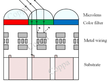
CMOS sensors in the market are categorized into three structures: front-illuminated (FSI), back-illuminated (BSI), and stacked (Stack). In a typical CMOS composition, components include microlenses, color filters, metal cables, photodiodes, and substrates.
In the front-illuminated (FSI) technology, light enters between the metal cables on the front and is focused on the photodiode. However, this approach may result in light reflection by the metal cable layer, leading to a reduced absorption of light by the photodiode and potential color distortion due to cross-talk with neighboring pixels.
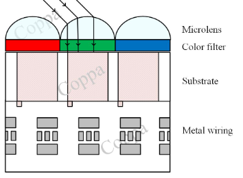
On the other hand, back-illuminated (BSI) technology constructs pixels without requiring light to pass through the metal wiring layer. This design allows light to reach the photodiode with minimal obstruction and interference, resulting in a highly efficient utilization of incident light.
The stacked (Stack) structure, first employed in SONY's Exmor RS products, separates the pixel and circuit areas. This enables the independent optimization of the pixel part for high image quality and the circuit part for enhanced performance. The stack structure inherits the advantages of back-illuminated types while overcoming production limitations and defects.
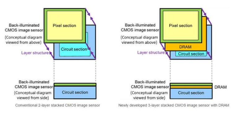
As processing circuits advance, cameras equipped with CMOS sensors can offer additional functionalities such as hardware HDR and slow-motion shooting. The independent optimization of pixel and circuit areas allows for smaller camera sizes without compromising functions or performance. Moreover, the flexibility to increase the pixel area (CMOS size) allows for planting more or larger pixels, contributing to improved image quality.
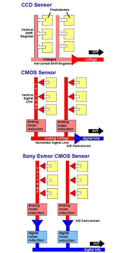
CCD vs CMOS: Working Diagram
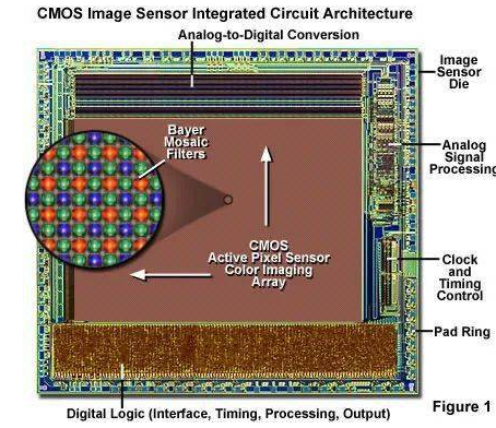
CMOS diagram: pixels, digital logic circuits, signal processors, clock controllers, etc.
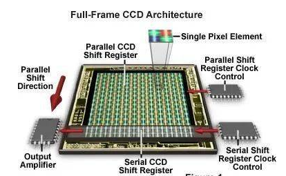
CCD Diagram: Horizontal and Vertical Shift Register, Clock Controller for Horizontal and Vertical Shift Register, Output Amplifier etc.

CCD sensor circuit diagram: Voltage conversion must occur after the charge is transferred to the horizontal shift register.

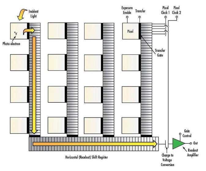
Schematic diagram of CMOS sensor: Each pixel contains a photosensitive element and a voltage converter, which can convert photons into voltage within the pixel.
If we ignore the circuit board and only focus on the photosensitive part, there is a schematic diagram as follows.
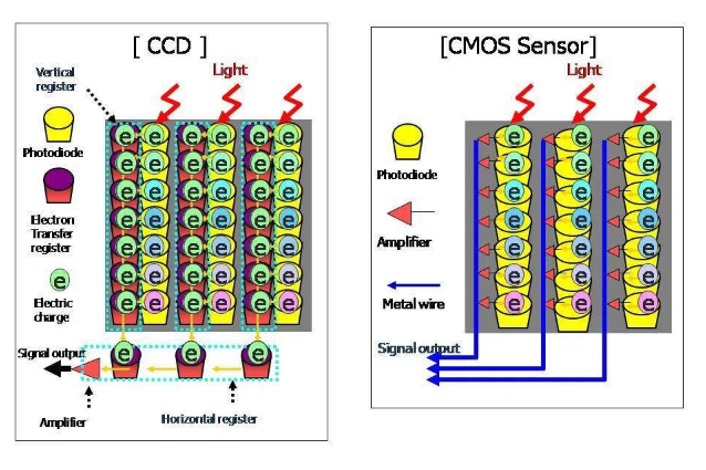
CCD
A CCD is essentially a large array of semiconductor "barrels" that convert incoming photons into electrons and hold the accumulated charge. These charges, can be transferred down by the vertical shift register to the horizontal shift register, which converts the charge into voltage and outputs it.

CMOS
Instead of transporting a bucket of charge, complementary metal-oxide semiconductors instantly convert the charge into voltage and output the voltage on a microwire.
CCD vs CMOS: Main Difference
The main distinction between CCD and CMOS sensors lies in the way they handle each pixel. In CCD, light-generated charge is moved from one pixel to another, and it is then converted into voltage at the output node. On the other hand, CMOS imagers use multiple transistors on each pixel to convert the charge within each pixel into voltage, employing a more traditional approach of amplifying and moving charges using wires.
The charge generated by CCD pixels needs to be initially stored in a vertical register, then transferred row by row to a horizontal register. Finally, the charge of each pixel is individually measured and the output signal is amplified. In contrast, CMOS sensors can generate voltage at each pixel, allowing for faster transmission through metal lines to the amplifier for output.
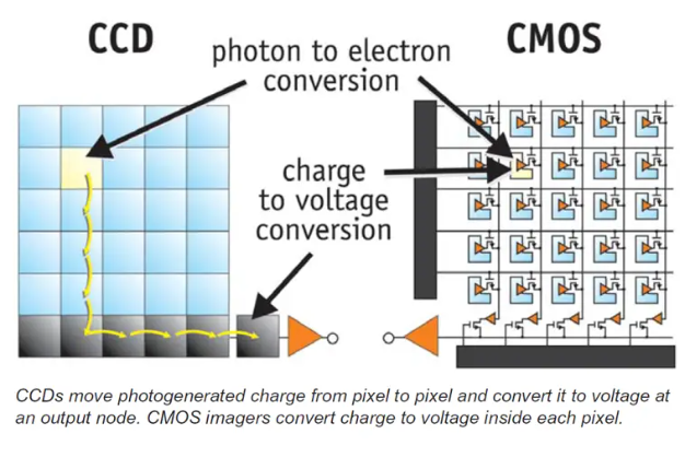
CCD moves light-generated charges from one pixel to another, converting them into voltage at the output node. In contrast, CMOS imagers use multiple transistors on each pixel to convert the charge within each pixel into voltage, employing a more traditional approach of amplifying and moving charges using wires.
CCD vs CMOS Sensor: Image Quality
CCD charge-coupler production technology has a long and mature history. It utilizes PN junctions or silicon dioxide (SiO2) isolation layers to effectively isolate noise, providing certain advantages in imaging quality compared to CMOS photoelectric sensors. The CMOS photoelectric sensors, due to their high integration level, have closely positioned photoelectric sensing elements and circuits. This proximity leads to significant optical, electrical, and magnetic interference, resulting in substantial noise that adversely affects image quality. This interference has historically limited the utility of CMOS photoelectric sensors. However, recent years have witnessed continuous advancements in CMOS circuit noise reduction technology, creating favorable conditions for the production of high-density and high-quality CMOS image sensors.
CCD vs CMOS: ISO Sensitivity
CMOS sensitivity is lower than that of CCD due to the complexity of each CMOS pixel, consisting of four transistors, a photosensitive diode, amplifiers, and digital-to-analog conversion circuits.
CCD vs CMOS: Resolution
The complexity of CMOS pixels makes it challenging to achieve the pixel size of CCD sensors, resulting in better resolution for CCD sensors of the same size.
CCD vs CMOS: Noise
CMOS sensors tend to have higher noise levels compared to CCD sensors due to the need for multiple amplifiers for each photosensitive diode.
CCD vs CMOS: Power Consumption
CMOS operates with active image acquisition, directly amplifying and outputting charge generated by photosensitive diodes. In contrast, CCD relies on passive acquisition, requiring charges to move to the transmission channel externally. The power consumption of CMOS is significantly lower (1/8 to 1/10) compared to CCD.
CCD vs CMOS: Cost
CMOS sensors, using the common CMOS process for semiconductor circuits, easily integrate peripheral circuits into the sensor, reducing costs. CCD, relying on charge transfer for data transmission, faces challenges in yield rates, making CCD sensors more expensive to manufacture than CMOS sensors.
CCD vs CMOS: Backup Camera/Reverse Camera
When comparing CCD and CMOS technologies in the context of backup cameras, which are commonly used in vehicles for assistance in parking and rearview monitoring, several factors come into play.
|
Criteria |
CCD |
CMOS |
|
Low Light Performance |
Traditionally superior, excelling in low-light conditions with clearer images and less noise. |
Historically considered less adept, but modern CMOS sensors provide satisfactory performance even in challenging lighting conditions. |
|
Image Quality |
Often associated with high-quality images, particularly in color accuracy and clarity. May excel in capturing intricate details. |
Significant strides in image quality; differences may be negligible for everyday use. Higher-end CMOS sensors can offer excellent image quality. |
|
Power Consumption |
Generally consumes more power, which may be a consideration for applications where energy efficiency is crucial. |
Known for lower power consumption, contributing to energy efficiency and potentially longer battery life in vehicles. |
|
Cost |
Historically more expensive to manufacture, potentially impacting overall backup camera costs. |
Generally more cost-effective, making CMOS-based backup cameras more affordable for consumers. |
|
Dynamic Range |
Often has a broader dynamic range, allowing for the capture of details in both bright and dark areas of an image. |
Advances in CMOS technology have improved dynamic range capabilities, although differences may exist in certain scenarios compared to CCD sensors. |
CCD vs CMOS: Color
|
Criteria |
CCD |
CMOS |
|
Color Accuracy |
Traditionally known for excellent color accuracy, providing precise reproduction. Suitable for applications where color fidelity is critical. |
Made significant strides in color accuracy. Modern CMOS sensors achieve high color accuracy comparable to CCD. |
|
Color Saturation |
Capable of producing saturated and vibrant colors. Known for capturing a wide range of colors with high saturation. |
Can deliver vibrant colors. Advancements in technology improve color reproduction, allowing for vivid and saturated images. |
|
Low Light Color Performance |
Traditionally strong in low-light conditions. Color performance remains consistent even in challenging lighting situations. |
Historically faced challenges in low-light color accuracy, but improvements have been made. Modern CMOS sensors provide satisfactory low-light color performance. |
|
Color Noise |
Known for producing low noise in color images. Well-established technology minimizes color artifacts. |
May exhibit slightly higher color noise, especially in earlier models. Advances have reduced the gap, and high-end CMOS sensors offer excellent color clarity. |
|
Dynamic Range and Color Gradients |
Often has a broad dynamic range, capturing subtle color gradients and details in both highlights and shadows. |
Advances in technology have improved dynamic range capabilities. Modern CMOS sensors capture a wide range of colors and subtle gradients. |
CCD vs APS-C
CCD and APS-C are not directly comparable, as one refers to sensor technology, and the other refers to a sensor size standard. APS-C sensors, which can use various technologies including CCD or CMOS, are commonly found in modern digital cameras, providing a good balance between image quality and camera size.
CCD vs CMOS: FPV Cameras
CCD FPV Cameras
CCD cameras excel in delivering high-quality images with accurate colors and low noise, making them a preferred choice when image clarity is crucial.
Many CCD cameras feature a global shutter, capturing the entire image simultaneously. This is advantageous in fast-paced activities like drone racing, preventing the rolling shutter effect.
Traditionally, CCD cameras exhibit strong performance in low-light conditions, providing clear images with minimal noise even in challenging lighting situations.
CCD cameras may offer lower latency compared to some CMOS cameras. This is important in FPV applications where real-time feedback is crucial for optimal performance.
CMOS FPV Cameras
Modern CMOS cameras have undergone significant advancements, narrowing the gap in image quality compared to CCD counterparts.
CMOS sensors are generally smaller and lighter, making CMOS FPV cameras a preferred choice for applications where compact size and low weight are critical, such as in racing drones.
CMOS cameras can provide a wide dynamic range, capturing details in both bright and dark areas. This contributes to enhanced overall image quality.
CMOS technology is typically more cost-effective, making CMOS-based FPV cameras more affordable without compromising on performance.
CCD vs CMOS: Pros and Cons
|
Aspect |
CCD |
CMOS |
|
Full Name |
Charge-Coupled Device |
Complementary Metal-Oxide-Semiconductor |
|
Definition |
A sensor technology that transfers charge between pixels for image capture. |
A sensor technology using metal-oxide-semiconductor components for image capture. |
|
Pixel Signal |
Charge transfer between pixels. |
Voltage signal directly read from each pixel. |
|
Image Quality |
Pros: High image quality with good color accuracy and low noise. |
Pros: Advances have narrowed the gap; modern CMOS can provide excellent image quality. |
|
Cons: Limited dynamic range in some cases. |
Cons: Historically had challenges, but improvements have addressed many issues. |
|
|
Resolution |
Generally lower resolution compared to CMOS. |
Often supports higher resolutions. |
|
Processing Speed |
Slower readout speeds. |
Faster readout speeds; suitable for high-speed applications like video recording. |
|
Noise |
Typically lower noise levels. |
Can exhibit noise in low-light situations, although improvements have been made. |
|
Sensitivity to Light |
Traditionally strong performance in low-light conditions. |
Advances in technology; many CMOS sensors offer good low-light performance. |
|
Energy Consumption |
Generally consumes more power. |
Lower power consumption, contributing to energy efficiency. |
|
Fever |
May produce more heat. |
Tends to heat up less, but power efficiency depends on specific designs. |
|
Cost |
Historically more expensive to manufacture. |
Generally more cost-effective; easier integration of peripheral circuits. |
|
Shutter |
Often features a global shutter. |
Can have a global shutter, but not universal; some CMOS sensors use rolling shutters. |
|
Difficulty in Manufacturing |
May have higher manufacturing complexities. |
Generally less challenging to manufacture, contributing to cost-effectiveness. |
Final Words
In the realm of imaging technology, the CCD (Charge-Coupled Device) and CMOS (Complementary Metal-Oxide-Semiconductor) sensors have been longstanding contenders, each with its unique strengths. The decision between CCD and CMOS involves a careful consideration of factors such as image quality preferences, low-light performance requirements, budget constraints, and the need for specific features like global shutter or high-speed capabilities. As technology continues to evolve, the distinctions between these two technologies are becoming less pronounced.
Read More:
Throttle Position Sensor Diagram
Crankshaft Position Sensor Location
Temporary Fix for Crankshaft Position Sensor
How to Test Crankshaft Sensor with Multimeter
Where Is the Knock Sensor Located
How to Start a Car with a Bad Crankshaft Sensor
How to Start a Car with a Bad Crankshaft Sensor
How does the Oxygen Sensor OSS-2 Effectively Improve Vehicle Exhaust Pollution Emissions
Where are Radar Sensors on Mercedes
How Many Sensors Are In a Car【Types & Functions】
How to Delete O2 Sensors from ECM
How Many O2 Sensors Does a Car Have
4 Wire Oxygen Sensor Wiring Diagram
Can a Bad O2 Sensor Cause a Misfire
How to Reset a Mass Air Flow Sensor
Can I Use a Downstream Oxygen Sensor for Upstream
Previous: What is a TMAP Sensor
Next: Size of Image Sensor: How Does Sensor Size Affect Image Quality
 FAQ
FAQ
- What are the types of digital cameras?
- The four main types of digital cameras are Digital Single-Lens Reflex (DSLR) cameras, point-and-shoot cameras, bridge cameras, and camera phones. DSLR cameras offer advanced features, interchangeable lenses, and optimal image quality but tend to be more expensive and larger in size. Point-and-shoot cameras are compact and easy to use, making them suitable for casual photographers. Bridge cameras bridge the gap between point-and-shoot and DSLR cameras, offering versatile features and a fixed, often powerful, zoom lens. Camera phones, integrated into smartphones, provide convenient and portable photography solutions but may have limitations in terms of image quality compared to dedicated cameras.
- Is CCD more sensitive to light?
- In general, monochrome CCD sensors are considered more light-sensitive than color sensors, including both OSC CCD and CMOS sensors. This heightened sensitivity is attributed to the fact that monochrome CCD pixels capture the entire spectrum of light without the hindrance of color filters, allowing each pixel to receive 100% of the incident light. In contrast, color sensors experience a reduction in sensitivity due to the presence of color filters, which limit the light reaching individual pixels. While advancements in technology have improved the sensitivity of color sensors, the absence of color filters remains a distinguishing factor that contributes to the higher overall sensitivity of monochrome CCD sensors.
- Is A CMOS sensor analog or digital?
- A CMOS (Complementary Metal-Oxide-Semiconductor) sensor, which is a type of active-pixel sensor, primarily operates in both the analog and digital domains. Analog Domain: Similar to CCD (Charge-Coupled Device) sensors, CMOS sensors start their operation in the analog domain. When light strikes the photosensitive elements (pixels) on a CMOS sensor, it generates an electrical charge. This charge is initially an analog signal and is directly proportional to the intensity of the incident light. Digital Domain: After the analog charge is generated, CMOS sensors use an analog-to-digital converter (ADC) to convert the analog signal into a digital one. This digital representation allows for subsequent digital processing, storage, and transmission of the image data.
- Is CCD analog or digital?
- CCD (Charge-Coupled Device) technology primarily operates in the analog domain. While it is common for people to associate CCD with digital devices, the misconception likely arises from the fact that CCDs are often used in conjunction with digital systems for signal processing and readout. The misconception may also stem from the fact that CCDs are frequently used in digital imaging applications. In such cases, the analog signal generated by the CCD is subsequently converted to a digital format through an analog-to-digital converter (ADC) during the readout process. This digital conversion facilitates further processing, storage, and manipulation of the image data by digital devices and systems.
- Is a DSLR a CCD or CMOS?
- In Digital Single-Lens Reflex (DSLR) cameras, the imaging sensors used are predominantly CMOS (Complementary Metal-Oxide-Semiconductor). While CCD (Charge-Coupled Device) sensors were more common in the early days of digital photography, the majority of modern DSLRs utilize CMOS technology. As technology has advanced, CMOS sensors have become the standard choice in DSLRs.
- Does Canon use CCD or CMOS?
- CMOS sensors
- Are CCD sensors still used?
- While CCD (Charge-Coupled Device) sensors were once the primary choice in various devices, their prevalence has diminished over time, giving way to image sensors based on complementary metal-oxide-semiconductor (CMOS) technology. CMOS sensors have gained prominence due to their advantages such as faster readout speeds, lower power consumption, and cost-effectiveness. Despite this shift, CCD sensors are not entirely obsolete. They still find application in specific scenarios where their unique features, such as superior image quality and a global shutter, are essential. Industries like astronomy, scientific imaging, and some specialized cameras may continue to utilize CCD sensors for their specific advantages. However, in many mainstream consumer devices and applications, CMOS sensors have become the dominant choice due to their overall efficiency and versatility.
- Are phone cameras CCD or CMOS?
- CMOS sensors
- Why did CMOS replace CCD?
- CMOS sensors replaced CCD sensors primarily due to their faster readout speeds, enabling higher video frame rates, and superior dynamic range, capturing a broader spectrum of tones. Additionally, CMOS sensors consume less power, making them energy-efficient, and their cost-effective manufacturing processes contributed to their widespread adoption. The ability to integrate peripheral circuits directly into the sensor chip, coupled with their versatility and smaller size, further solidified CMOS sensors as the preferred choice across various applications, including portable devices and imaging systems requiring compact designs.
- Which is better, CCD vs CMOS?
- CCD sensors, historically recognized for superior image quality and a global shutter, are favored in applications where these features are critical. On the other hand, CMOS sensors offer higher resolution, faster readout speeds, and lower power consumption, making them a cost-effective and versatile choice for various scenarios.
Latest Blogs
Popular Manufacturers