
Everything You Need for Automotive Chips & Parts Assembly.
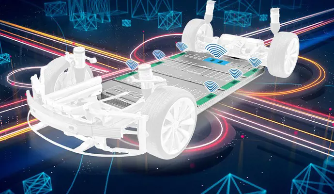
With a wealth of data analysis and research in the field of automotive electronics, Nevsemi enables customers to design high-reliability solutions that create value for the end-user.

A comprehensive range of automotive-grade semiconductor products for critical automotive electronic systems.

Active suspension can take into account the smoothness and handling stability of the car, while in the traditional passive suspension design, smoothness and handling stability are often difficult to take into account, and generally have to take a compromise approach.When the load quality changes or road conditions change, the active suspension can ...
IVI can realize a series of applications including 3D navigation, real-time road conditions, IPTV, assisted driving, fault detection, vehicle information, body control, mobile office, wireless communication, online-based entertainment functions and TSP services, which greatly enhance the level of vehicle electronics, networking and intelligence. Ne...


The power system of a car is the whole process of mechanical arrangement in which the power generated by the engine is transmitted to the wheels through a series of power transmissions. The engine runs, in fact, the crankshaft is rotating, and one end of the crankshaft ...

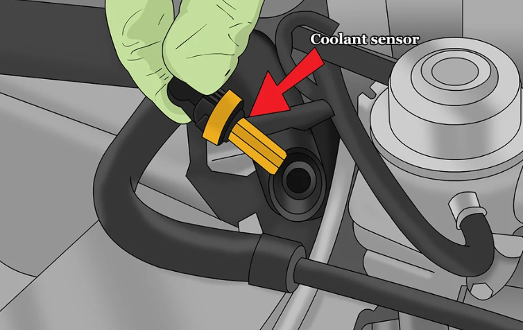
How to Replace a Coolant Temperature Sensor
The coolant temperature sensor is a critical component of a vehicle's engine management system, responsible for monitoring the temperature of the engine coolant. Over time, these sensors can wear out or malfunction, leading to inaccurate temperature readings and potential issues with engine performance. In this guide, we will explore the process of replacing a coolant temperature sensor, outlining the steps involved and providing valuable tips to ensure a successful replacement. By following these instructions, vehicle owners can maintain the proper functioning of their engine cooling system and prevent potential damage to their vehicles.
What is a coolant temperature sensor?
A coolant temperature sensor, also known as a water temperature sensor, is a crucial component in a vehicle's engine cooling system. Its primary function is to monitor the temperature of the engine coolant. The engine coolant is a mixture of water and antifreeze that circulates through the engine to regulate its temperature and prevent overheating.
The coolant temperature sensor measures the temperature of the coolant and sends this information to the engine control unit (ECU) or engine control module (ECM) of the vehicle. The ECU uses this data to adjust various engine parameters to ensure optimal performance and efficiency.
Coolant Temperature Sensor Working Principle
The principle behind the coolant temperature sensor involves the utilization of a thermistor with a negative temperature coefficient (NTC). In summary, the coolant temperature sensor operates on the principle of using an NTC thermistor to measure the temperature of the engine coolant. The sensor's output voltage varies with changes in coolant temperature, allowing the ECU to make real-time adjustments to engine parameters for optimal performance, fuel efficiency, and emissions control.
Thermistor Construction: Inside the coolant temperature sensor, there's a thermistor—a type of resistor whose electrical resistance varies with temperature. In the case of the coolant temperature sensor, it's typically an NTC thermistor. NTC thermistors have a characteristic where their resistance decreases as the temperature increases, and vice versa.
Contact with Coolant: The slender head of the sensor is immersed in the engine coolant, ensuring direct contact with the fluid. As the engine runs and heats up, the temperature of the coolant rises.
Resistance Variation: As the temperature of the coolant increases, the resistance of the NTC thermistor inside the sensor decreases. This change in resistance is proportional to the temperature of the coolant. Conversely, as the coolant temperature decreases, the resistance of the thermistor increases.
Output Voltage Change: The coolant temperature sensor is connected to the engine control unit (ECU) or engine control module (ECM) of the vehicle. It sends an electrical signal to the ECU, which corresponds to the resistance of the thermistor. This signal is typically a voltage that varies depending on the resistance of the thermistor. As the resistance changes with the temperature of the coolant, so does the voltage output from the sensor.
ECU Adjustment: The ECU receives the voltage signal from the coolant temperature sensor and interprets it as the temperature of the engine coolant. Based on this temperature data, the ECU adjusts various engine parameters such as fuel injection timing, fuel injection quantity, ignition timing, and idle speed control.
Fuel Injection and Ignition Timing Correction: By accurately monitoring the coolant temperature, the ECU can optimize the fuel-air mixture and ignition timing for efficient combustion under different operating conditions. For example, during cold starts, the ECU may enrich the fuel mixture and adjust the ignition timing to aid in starting the engine smoothly.
How to Replace a Coolant Temperature Sensor?
Replacing a coolant temperature sensor involves several steps to ensure safe and proper installation. Here's a detailed guide:
Preparing the Right Tools:
Socket wrench set
Drain pan
Screwdriver
Jack stands
Funnel
Pliers
Procedure:
Let the Engine Cool:
Allow the engine to cool down for at least an hour before starting work.
Disconnect the Battery:
Disconnect the negative terminal of the car battery to ensure safety during the procedure.
Wear Safety Equipment:
Wear gloves and goggles to protect yourself from hot coolant.
Locate the Sensor:
The coolant temperature sensor is typically near the radiator or thermostat housing in front of the engine. Refer to a repair manual for specific guidance.
Remove Engine Cover (if necessary):
Use a wrench to remove nuts and bolts securing the engine cover, if applicable.
Drain Coolant:
Drain coolant from the cooling system to prevent spillage when removing the sensor.
Disconnect Sensor Wiring Connector:
Carefully disconnect the wiring connector from the sensor.
Use a Ratchet Wrench:
Use a ratchet wrench to loosen the sensor. Apply release spray if necessary.
Clean Threads:
Clean the threads where the sensor is installed to remove debris.
Install New Sensor:
Hand-twist the new sensor into place, ensuring proper alignment of threads.
Use a torque wrench to tighten the sensor to the manufacturer's specified torque.
Reconnect Wiring Harness:
Clean the sensor's connector before plugging it in to ensure a good connection.
Refill Cooling System:
Refill the cooling system with coolant.
Check for Leaks:
Check for any leaks around the new sensor.
Reconnect Battery:
Reconnect the car battery.
Test Operation:
Start the engine and ensure proper operation. The vehicle's PCM should receive correct temperature information.
By following these steps carefully, you can safely replace the coolant temperature sensor and ensure the proper functioning of your vehicle's engine cooling system. If you're unsure about any step, it's always recommended to consult a professional mechanic or refer to a repair manual for specific guidance.
Is the coolant temperature sensor easy to replace?
While replacing a coolant temperature sensor may seem straightforward, it's essential to approach the task with caution due to the potential dangers associated with working around hot coolant. Here are some points to consider regarding the ease and safety of replacing the coolant temperature sensor.
Ease of Replacement:
Simple Procedure:
Generally, the procedure to replace a coolant temperature sensor involves unscrewing the sensor from its socket, disconnecting the wiring, and installing the new sensor.
It usually doesn't require complex tools or specialized knowledge, making it relatively easy for DIY enthusiasts.
Accessible Location:
Coolant temperature sensors are typically located near the radiator or thermostat housing, making them relatively accessible for replacement.
Safety Considerations
Hot Coolant Hazard:
The primary danger associated with replacing the coolant temperature sensor is the risk of coming into contact with hot coolant.
Hot coolant can cause severe burns if it splashes onto the skin or eyes, making it crucial to allow the engine to cool down before attempting the replacement.
Cooling Down Period:
Before replacing the sensor, it's essential to let the vehicle sit and cool down with the radiator cap off to release built-up pressure and prevent the sudden release of hot coolant.
Allowing the engine to cool reduces the risk of burns and makes the replacement process safer.
Proper Safety Gear:
Wearing appropriate safety gear such as gloves and goggles can provide added protection against hot coolant splashes.
While the actual process of replacing the coolant temperature sensor may be straightforward, it's essential to prioritize safety and take precautions to avoid potential hazards associated with working around hot coolant.
With proper safety measures in place, DIY enthusiasts or individuals with basic mechanical knowledge should be able to replace the coolant temperature sensor without significant difficulty.
How long does it take to replace a coolant temperature sensor?
The time it takes to replace a coolant temperature sensor can vary depending on factors such as the vehicle model, accessibility of the sensor, and the experience level of the person performing the replacement.
In summary, while the actual process of removing and replacing the coolant temperature sensor may only take around 5-10 minutes, additional factors such as preparation, draining coolant, testing, and cleanup can extend the total time to complete the job. On average, the entire process may take anywhere from 30 minutes to an hour or more, depending on the specific circumstances.
Do you need to drain coolant to change the coolant temperature sensor?
While it's possible to replace the coolant temperature sensor without draining coolant, it's generally safer and more practical to drain some coolant beforehand to minimize the risk of coolant loss and ensure a smoother replacement process.
How much does it cost to replace a coolant temperature sensor?
Replacing a coolant temperature sensor typically costs between $399 and $441. This price range includes both the cost of the part itself, which can range from $5 to $250, and the labor costs, which are usually between $100 and $150.
Here's a breakdown of the costs:
Parts: $5 - $250
Labor: $100 - $150
However, it's important to remember that this is just a general estimate. The actual cost can vary depending on several factors, such as:
The make and model of your car: Coolant temperature sensors for certain luxury or high-performance cars may be more expensive than those for common vehicles.
Your location: Labor rates can vary depending on your geographic area.
The repair shop you choose: Different mechanics will have different rates.
Is it OK to drive with a bad coolant temp sensor?
Driving with a faulty engine coolant temperature sensor is not recommended due to the risk of running the engine too rich, leading to poor fuel economy, increased emissions, engine performance issues, potential damage to engine components, and costly repairs. It's advisable to promptly address any issues with the coolant temperature sensor to ensure proper engine operation and avoid further damage.
How do I know if my coolant temp sensor is bad?
There are several signs that may indicate a faulty coolant temperature sensor.
Engine Temperature Gauge: If the engine temperature gauge on your dashboard reads abnormally high or fluctuates erratically, it could be a sign of a malfunctioning coolant temperature sensor.
Check Engine Light: A faulty coolant temperature sensor can trigger the check engine light to illuminate on your dashboard. You can use an OBD-II scanner to retrieve the trouble codes stored by the vehicle's computer, which may provide information about the issue.
Poor Fuel Economy: A malfunctioning coolant temperature sensor can cause the engine to run too rich or too lean, leading to decreased fuel efficiency.
Rough Idling or Stalling: Incorrect temperature readings from the coolant temperature sensor can result in improper fuel mixture adjustments, causing the engine to idle roughly or stall.
Difficulty Starting: If the coolant temperature sensor provides inaccurate readings, it can affect the engine's ability to start, especially in cold or hot conditions.
Excessive Emissions: A faulty coolant temperature sensor can cause the engine to run too rich, leading to increased emissions of pollutants such as hydrocarbons (HC) and carbon monoxide (CO).
Overheating: In some cases, a malfunctioning coolant temperature sensor may fail to properly detect overheating, leading to potential engine damage if the issue is not addressed promptly.
Will a coolant temp sensor throw a code?
Yes, a faulty coolant temperature sensor can trigger a diagnostic trouble code (DTC) to be stored in the vehicle's engine control module (ECM) or powertrain control module (PCM). One common DTC associated with a malfunctioning coolant temperature sensor is P0115, which indicates an Engine Coolant Temperature (ECT) sensor malfunction.
Where is the coolant temperature sensor located?
The exact location of the coolant temperature sensor can vary depending on the make and model of the vehicle. However, it is typically located somewhere near the engine coolant passages to accurately measure the temperature of the coolant.
Near the Cylinder Head: As you mentioned, the coolant temperature sensor is often located near the cylinder head, where it can directly sense the temperature of the coolant as it flows through the engine.
On or Near the Thermostat Housing: The thermostat housing is another common location for the coolant temperature sensor, as it is close to the engine block and allows for easy access to the coolant passages.
Near the Radiator: In some vehicles, especially those with transverse-mounted engines, the coolant temperature sensor may be located near the radiator or coolant hoses, where it can measure the temperature of the coolant as it enters or exits the radiator.
On the Engine Block: Occasionally, the coolant temperature sensor may be mounted directly on the engine block itself, particularly in older or simpler engine designs.
Underneath the Intake Manifold: In certain engine configurations, such as V-type engines, the coolant temperature sensor may be located underneath the intake manifold, making it more challenging to access.
What is the difference between a coolant temperature sensor and a coolant temperature switch?
In modern automotive terminology, the terms "coolant temperature sensor" and "coolant temperature switch" are often used interchangeably to refer to the same component: a sensor that measures the temperature of the engine coolant.
What is the code for a bad coolant sensor?
The P0128 code specifically indicates that the engine coolant temperature (ECT) sensor is reading a temperature below the expected threshold for the engine operating conditions. This can suggest that the engine is not reaching the proper operating temperature within a specified time frame, which could be caused by various factors, including a malfunctioning coolant temperature sensor.
Final Words
Replacing a coolant temperature sensor is a relatively straightforward task that can be completed with the right tools and knowledge. By following the steps outlined in this guide, vehicle owners can address issues with faulty or malfunctioning coolant temperature sensors, ensuring accurate temperature readings and optimal engine performance.
Mar 14, 2024
How to Reset a Coolant Temperature Sensor

You might be frustrated with your engine temperature gauge acting up, only to find suggestions about resetting the electronic coolant temperature sensor (ECT).
However, here's the truth: resetting the ECT won't resolve anything. Why? Because the ECT isn't like your computer or smartphone—it's a humble resistor without any fancy computing power. Therefore, resetting it won't magically fix any malfunctions. If your ECT is on the fritz, the best course of action is to replace it.
The Role of Coolant Temperature Sensor in Engine Management
The coolant temperature sensor, often abbreviated as ECT or CTS, is a crucial component of the engine management system in modern vehicles.
Its primary function is to monitor the temperature of the engine coolant and provide this data to the engine control unit (ECU) or engine control module (ECM).
The ECU uses the temperature information from the coolant sensor to adjust various engine parameters, such as fuel injection timing, ignition timing, and idle speed, to ensure optimal engine performance and efficiency across different operating conditions.
Coolant Temperature Sensor Operation
The coolant temperature sensor operates based on the principle of electrical resistance variation with temperature changes.
It is typically a negative temperature coefficient (NTC) thermistor, meaning its electrical resistance decreases as the temperature increases.
As the engine warms up, the resistance of the sensor decreases, allowing more current to flow through it. The ECU interprets this change in resistance to determine the coolant temperature.
Can you reset a coolant temp sensor
No, it's not possible to reset a coolant temperature sensor.
Why You Can't Reset a Coolant Temperature Sensor
Unlike electronic components with memory or software, such as microcontrollers or sensors in more complex systems, the coolant temperature sensor does not store any data or have any inherent memory.
Resetting a component typically involves clearing stored data or resetting software parameters to default settings. Since the coolant temperature sensor doesn't store any data or have software, there's nothing to reset.
The functionality of the sensor is purely based on its physical characteristics (i.e., resistance changes with temperature) and its interaction with the ECU.
Interaction with the Engine Control Unit (ECU)
The ECT communicates with the ECU through electrical signals. The ECU sends a regulated voltage (typically 5 volts) to the sensor, and the sensor's output voltage varies depending on the coolant temperature.
This voltage signal is then interpreted by the ECU to determine the engine's operating temperature, which is crucial for making real-time adjustments to engine parameters.
Diagnosing Coolant Temperature Sensor Issues:
While the coolant temperature sensor itself cannot be reset, it can malfunction over time due to factors such as age, contamination, or electrical issues.
Common symptoms of a faulty coolant temperature sensor include inaccurate temperature readings, poor engine performance, difficulty starting the engine when cold, or illuminated dashboard warning lights.
Diagnosing sensor issues typically involves testing its resistance or voltage output using a multimeter, and comparing the readings with manufacturer specifications.
Understanding the operation and limitations of the coolant temperature sensor is essential for diagnosing and resolving engine performance issues effectively. While it cannot be reset like some electronic components, proper diagnosis and replacement when necessary are crucial for maintaining optimal engine performance and efficiency.
Indications of a Faulty Coolant Temperature Sensor
Difficulty Starting the Engine When Cold
During cold starts, engines require extra fuel to maintain operation until they reach optimal temperature. However, if the engine coolant temperature (ECT) sensor malfunctions, the engine control unit (ECU) struggles to gauge the temperature accurately, resulting in insufficient fuel injection.
This can lead to difficulties in starting the engine, irregular idling, or sluggish acceleration.
It's worth noting that while ECT malfunctions could cause these issues, other factors like faulty fuel injectors, a broken idle air control valve, or leaks in the exhaust gas recirculation system could also be contributing factors.
Anomalies in the Engine Temperature Gauge
Typically, a fully functional engine heats up to the middle of the temperature range on the gauge and remains stable. However, when the ECT sensor malfunctions, the engine temperature gauge may display erratic readings.
You might notice the gauge indicating overheating when the engine is started, or it might remain cool while driving.
If you observe the gauge needle remaining stationary throughout your drive without any noticeable engine performance issues, it's possible that the problem lies with the temperature gauge itself rather than the engine components.
Decreased Fuel Efficiency
A sudden drop in fuel mileage could signal a malfunctioning ECT sensor. When the engine is cold, the ECU relies heavily on data from the ECT sensor to determine fuel injection rates.
If the sensor fails to provide accurate temperature readings, the ECU may inject either too much or too little fuel, resulting in decreased fuel efficiency.
However, it's essential to consider other potential causes such as faulty injectors, malfunctioning oxygen sensors, or even low tire pressure, which can also contribute to decreased mileage.
Abnormal Exhaust Characteristics
A malfunctioning ECT sensor can disrupt the fuel-air mixture in the combustion chamber, leading to excessive fuel injection.
Consequently, you may notice black smoke emanating from the exhaust or detect a strong odor of unburned fuel.
It's important to note that gassy-smelling exhaust can also stem from leaks in the exhaust system, so a thorough inspection is warranted.
Illumination of the Check Engine Light
If the check engine light illuminates and you suspect ECT sensor issues, it's advisable to visit an auto shop for code reading.
Common trouble codes associated with coolant temperature sensor malfunction include 17704 (error in the mapped cooling system), 01039 (ECT sensor RPM at idle is irregular), p1296 35-00 (ECT sensor or thermostat malfunction), and p0118/16502 (ECT sensor circuit high input).
Prompt diagnosis and resolution of these issues are crucial for maintaining engine performance and preventing further damage.
What to do after replacing the coolant temperature sensor?
Reconnect the Battery: Ensure the battery is securely reconnected to restore power to the vehicle's electrical systems. This step is crucial for the engine control unit (ECU) to recognize the new sensor and reset any stored error codes.
Check for "Check Engine" Light: Start the engine and observe the instrument cluster for the "check engine" light. If the replacement was successful, the light should go out shortly after starting the engine. If the light remains illuminated, there may be underlying issues that need further diagnosis.
Perform Coolant System Bleeding (if necessary): If a coolant flush was performed or if air was introduced into the cooling system during sensor replacement, it's essential to bleed the system to remove any trapped air pockets. Follow the manufacturer's guidelines or consult a repair manual for the proper bleeding procedure specific to your vehicle.
Monitor Temperature Gauge: Take the vehicle for a test drive while closely monitoring the temperature gauge on the instrument cluster. Ensure that the gauge registers the engine temperature accurately and remains within the normal operating range throughout the drive. Any abnormal fluctuations or indications of overheating should be addressed promptly.
Recheck Coolant Level: After a few days of driving, recheck the coolant level in the reservoir to ensure it remains at the recommended level. Top up the coolant if necessary to maintain proper engine cooling and prevent overheating.
Mar 04, 2024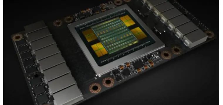
NVIDIA V100: The Most Advanced Data Center GPU
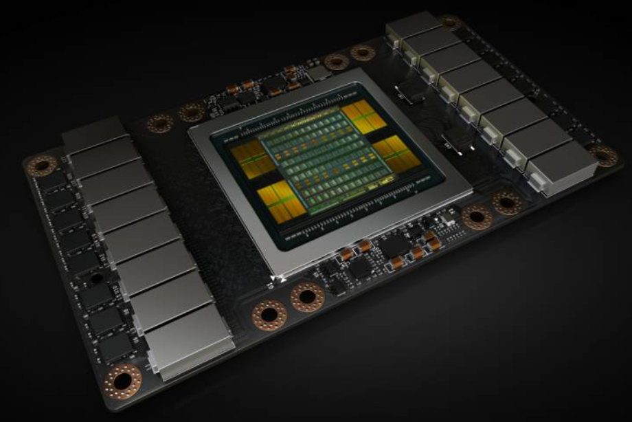
In the ever-evolving landscape of artificial intelligence (AI), the quest for high-performance computing solutions has become paramount. Among the myriad of options available, one name stands out: NVIDIA V100. Renowned for its exceptional capabilities, the NVIDIA V100 GPU (Graphics Processing Unit) has emerged as a game-changer, empowering researchers, scientists, and developers to push the boundaries of AI innovation.
Nvidia V100 SPECS
Architecture: NVIDIA Volta
CUDA Cores: 5120
Tensor Cores: 640
Memory:
Type: HBM2
Capacity: Available in 16GB and 32GB configurations
Memory Interface: 4096-bit
Memory Bandwidth: Up to 900 GB/s
Compute Performance:
Single-Precision (FP32): Up to 14.8 TFLOPS
Double-Precision (FP64): Up to 7.4 TFLOPS
Tensor Performance: Up to 125 TFLOPS (with Tensor Cores)
GPU Boost Clock: Up to 1530 MHz
Form Factor: PCIe (for PCIe version)
Interconnect: NVLink (for NVLink version)
Manufacturing Process: 12nm FinFET
Power Consumption:
Thermal Design Power (TDP): Approximately 250W
Maximum Power Consumption: Up to 300W
Cooling: Active cooling solutions (fans)
API Support: CUDA, DirectCompute, OpenCL
Supported Platforms:
Compatible with systems supporting PCIe or NVLink interconnects
Typically deployed in data center servers, workstations, and HPC clusters
Software Support: Compatible with NVIDIA CUDA Toolkit and associated software libraries for GPU-accelerated computing.
Nvidia V100 Release Date
The NVIDIA Tesla V100 GPU was officially announced by NVIDIA on May 10, 2017. It was later released on June 21, 2017. The Tesla V100 marked a significant milestone in GPU technology, introducing the powerful Volta architecture and setting new standards for performance, efficiency, and versatility in data center computing.
Nvidia V100 Memory
The NVIDIA V100 GPU utilizes High Bandwidth Memory 2 (HBM2) as its memory technology. HBM2 is a type of stacked memory that offers significantly higher bandwidth and lower power consumption compared to traditional GDDR5 memory. This advanced memory architecture allows the V100 to achieve faster data access speeds and better overall performance, making it well-suited for memory-intensive tasks such as deep learning training, scientific simulations, and high-performance computing (HPC) workloads. The V100 is available in configurations with either 16GB or 32GB of HBM2 memory, providing users with options to match their specific computational requirements and memory needs.
Nvidia V100 Cuda Cores
The NVIDIA V100 GPU features 5120 CUDA cores. These CUDA cores are the fundamental processing units responsible for executing parallel computations in GPU-accelerated applications. By leveraging parallelism, CUDA cores enable the V100 to perform highly efficient and massively parallel processing, making it ideal for demanding workloads such as artificial intelligence, deep learning, scientific computing, and high-performance computing (HPC). With its large number of CUDA cores, the V100 delivers exceptional computational power and performance, allowing users to tackle complex tasks with speed and efficiency.
What is the Nvidia V100 Used For
The NVIDIA® V100 Tensor Core stands as the epitome of innovation in the realm of data center GPUs, specifically engineered to accelerate a wide spectrum of tasks critical to modern computing. Leveraging the cutting-edge NVIDIA Volta architecture, the V100 is available in both 16 and 32GB configurations, offering computational capabilities equivalent to that of up to 32 CPUs housed within a single GPU.
Accelerating Artificial Intelligence (AI)
The Nvidia V100 is a cornerstone in the realm of artificial intelligence, acting as a catalyst for advancing AI research, development, and deployment. Its specialized Tensor Cores are tailored to accelerate deep learning workloads, facilitating rapid training and inference tasks in domains such as:
Natural Language Processing (NLP): Enabling the analysis and comprehension of human language, vital for applications like sentiment analysis, language translation, and chatbots.
Image Recognition: Powering computer vision applications, including object detection, image classification, and facial recognition, across diverse industries from healthcare to automotive.
Speech Recognition: Enhancing voice-enabled interfaces, virtual assistants, and speech-to-text systems by swiftly processing and interpreting audio data.
Empowering High Performance Computing (HPC)
In the realm of high-performance computing, the Nvidia V100 emerges as a cornerstone, revolutionizing the landscape with its unparalleled computational prowess. Capable of handling complex simulations and computations, the V100 is instrumental in:
Scientific Simulations: Facilitating intricate simulations in fields such as physics, chemistry, biology, and climate modeling, enabling researchers to unravel complex phenomena and drive scientific discovery.
Financial Modeling: Accelerating quantitative analysis, risk assessment, and algorithmic trading strategies in the finance industry, enhancing decision-making processes and optimizing investment strategies.
Drug Discovery: Powering molecular modeling and virtual screening techniques, expediting the discovery and development of novel therapeutics and pharmaceutical compounds to address pressing healthcare challenges.
Driving Data Science and Analytics
The Nvidia V100 plays a pivotal role in driving advancements in data science and analytics, empowering organizations to extract actionable insights from vast datasets with unprecedented speed and accuracy. Its robust computational capabilities enable:
Big Data Analytics: Processing and analyzing massive datasets with agility, uncovering hidden patterns, trends, and correlations to inform strategic decision-making and drive business growth.
Machine Learning: Training complex machine learning models on diverse datasets, enabling predictive analytics, recommendation systems, and anomaly detection across various domains, from e-commerce to cybersecurity.
Enhancing Graphics Workloads
Beyond its prowess in AI and HPC, the Nvidia V100 excels in enhancing graphics-intensive applications, delivering immersive visual experiences and enabling creative expression.
Rendering: Accelerating the rendering of photorealistic graphics, animation, and visual effects in industries spanning entertainment, architecture, and product design.
Visualization: Empowering real-time data visualization and immersive virtual environments for applications ranging from scientific visualization to architectural walkthroughs and industrial design.
In essence, the Nvidia V100 Tensor Core transcends the traditional boundaries of GPU computing, serving as a versatile powerhouse that drives innovation across AI, HPC, data science, and graphics. Its unmatched performance, powered by the NVIDIA Volta architecture, cements its position as the cornerstone of modern data center infrastructure, empowering organizations to tackle the most complex computational challenges and unlock new frontiers of discovery and innovation.
Key Features
Volta architecture: The Tesla V100 is based on the NVIDIA Volta architecture, which is designed for high performance and efficiency.
Tensor cores: The Tesla V100 includes 640 Tensor cores, which are designed to accelerate deep learning workloads.
HBM2 memory: The Tesla V100 is available with 16GB or 32GB of HBM2 memory, which provides high bandwidth and low latency.
High performance: The Tesla V100 can deliver up to 14.8 TFLOPS of single-precision performance and 125 TFLOPS of TensorFLOPS performance.
Large memory capacity: The Tesla V100 is available with 16GB or 32GB of memory, which is important for training large deep learning models.
Benefits
The NVIDIA Tesla V100 offers a number of benefits for data centers, including:
Accelerated AI: The Tesla V100 can significantly accelerate AI workloads, including deep learning training and inference.
Improved HPC performance: The Tesla V100 can also improve the performance of HPC workloads, such as scientific simulations and financial modeling.
Enhanced graphics: The Tesla V100 can also be used to enhance graphics workloads, such as rendering and visualization.
Performance
The NVIDIA Tesla V100 is a very powerful GPU. It can deliver up to 14.8 TFLOPS of single-precision performance and 125 TFLOPS of TensorFLOPS performance. This makes it ideal for a variety of demanding tasks, such as training deep learning models, running scientific simulations, and rendering complex graphics.
Nvidia v100 vs A100
The comparison between the Nvidia V100 and A100 GPUs is pivotal for users seeking optimal performance and efficiency in their computational endeavors. While both GPUs are formidable in their own right, the A100 introduces significant enhancements over its predecessor, the V100. Here's a closer look at how they stack up:
Performance
On the BERT (Bidirectional Encoder Representations from Transformers) benchmark, the A100 demonstrates remarkable performance gains over the V100. Specifically, the A100 outperforms the V100 by a staggering factor of 5x on the BERT TF32 benchmark and 2.5x on the BERT FP16 benchmark. This substantial improvement in performance positions the A100 as the preferred choice for users prioritizing swift neural network training and inference tasks.
Enhanced Specifications and Features
The A100 GPU boasts improved specifications and introduces innovative features that further elevate its performance and versatility. Notably, the A100 introduces TF32, a novel numerical format optimized for deep learning workloads. TF32 enables faster and more efficient training of neural networks, harnessing the full potential of the GPU's computational capabilities. Additionally, the A100 incorporates advancements in architecture and technology, enhancing its overall efficiency and efficacy in handling diverse computational tasks.
Implications for Users
For users engaged in deep learning and AI research, the A100 emerges as the superior choice, offering unparalleled performance and efficiency compared to the V100. Its ability to accelerate neural network training by a factor of 5x on the BERT TF32 benchmark and 2.5x on the BERT FP16 benchmark translates to significant time and cost savings, making it an invaluable asset for organizations seeking to stay at the forefront of AI innovation.
Conclusion
While the Nvidia V100 remains a formidable GPU in its own right, the A100 represents a significant leap forward in terms of performance, efficiency, and innovative features. With its superior computational capabilities and advancements in architecture, the A100 emerges as the preferred choice for users looking to maximize the speed and efficiency of their neural network training and inference tasks. As AI and deep learning continue to evolve, the A100 stands poised to redefine the landscape of GPU computing, driving innovation and breakthroughs across diverse industries and applications.
Nvidia V100 vs A6000
The NVIDIA V100 and A6000 are both powerful GPUs designed for different purposes, and there are significant differences between them.
Architecture:
The V100 is based on the Volta architecture, while the A6000 is based on the Ampere architecture. The Ampere architecture introduces several enhancements over Volta, including improved ray tracing capabilities, tensor core performance, and overall efficiency.
CUDA Cores and Tensor Cores:
The V100 features 5120 CUDA cores and 640 Tensor Cores.
The A6000 features 10752 CUDA cores and 336 Tensor Cores. This indicates a significant increase in computational power and AI performance in the A6000 compared to the V100.
Memory:
The V100 is available with either 16GB or 32GB of HBM2 memory.
The A6000 is equipped with 48GB of GDDR6 memory. While the A6000 offers more memory capacity compared to the V100, it uses GDDR6 memory instead of the HBM2 memory used in the V100.
Performance:
The A6000 generally offers higher performance compared to the V100, thanks to its newer architecture, higher CUDA core count, and enhanced tensor core performance.
The A6000 is particularly well-suited for AI and deep learning tasks due to its improved tensor core performance.
Use Cases:
The V100 is commonly used in data centers for AI training, scientific computing, and high-performance computing (HPC) tasks.
The A6000 is also suitable for data center deployments but is often used in workstations for professional visualization, AI development, and graphics-intensive tasks.
Price:
The A6000 is generally priced higher than the V100 due to its newer architecture, higher performance, and larger memory capacity.
Nvidia T4 vs V100
The NVIDIA T4 and V100 are both powerful GPUs designed for different purposes, and they have distinct differences.
Architecture:
The T4 is based on the Turing architecture, while the V100 is based on the Volta architecture. The Turing architecture introduces advancements in ray tracing, AI performance, and efficiency compared to the Volta architecture.
CUDA Cores and Tensor Cores:
The T4 features 2560 CUDA cores and 320 Tensor Cores.
The V100 features 5120 CUDA cores and 640 Tensor Cores. This indicates that the V100 offers higher computational power and AI performance compared to the T4.
Memory:
The T4 is available with 16GB of GDDR6 memory.
The V100 is available with either 16GB or 32GB of HBM2 memory. While the T4 offers higher memory capacity compared to the T4, it uses GDDR6 memory instead of the faster HBM2 memory used in the V100.
Performance:
The V100 generally offers higher performance compared to the T4, thanks to its higher CUDA core count, higher memory bandwidth, and larger memory capacity.
The V100 is particularly well-suited for demanding AI training, scientific computing, and high-performance computing (HPC) tasks.
Use Cases:
The T4 is commonly used in data centers for inference workloads, deep learning inference, and virtual desktop infrastructure (VDI).
The V100 is also used in data centers but is typically employed for AI training, scientific simulations, and HPC tasks that require higher computational power.
Price:
The T4 is generally priced lower than the V100 due to its lower computational power and memory capacity.
In summary, while both the NVIDIA T4 and V100 are powerful GPUs, the V100 offers higher computational power, memory bandwidth, and performance compared to the T4.
Nvidia Tesla V100 vs RTX 3090
Comparing the NVIDIA Tesla V100 and the RTX 3090 GPUs reveals differences in their architectures, features, and intended use cases. Here's a breakdown of their key distinctions:
Architecture:
The Tesla V100 is based on the Volta architecture, which is optimized for data center and high-performance computing (HPC) workloads.
The RTX 3090 is based on the Ampere architecture, designed for gaming, content creation, and AI workloads.
CUDA Cores:
The Tesla V100 features 5120 CUDA cores.
The RTX 3090 boasts 10496 CUDA cores, indicating a significantly higher number of cores compared to the V100.
Tensor Cores:
The Tesla V100 includes 640 Tensor Cores.
The RTX 3090 also incorporates Tensor Cores for AI and machine learning tasks, although the specific count is not directly comparable to the V100.
Memory:
The Tesla V100 offers up to 32GB of HBM2 memory with a memory bandwidth of up to 900 GB/s.
The RTX 3090 comes with 24GB of GDDR6X memory, offering faster memory speeds compared to the V100.
Performance:
The Tesla V100 is optimized for compute-intensive workloads such as deep learning training, scientific simulations, and HPC tasks. It excels in these areas with high compute performance and memory bandwidth.
The RTX 3090 is designed for gaming at 4K resolution, content creation, and AI inference tasks. While it offers impressive performance in gaming and AI applications, it may not match the V100 in terms of raw compute power for data center tasks.
Price:
The Tesla V100 is typically priced higher than consumer GPUs like the RTX 3090 due to its specialized design and intended use in data centers and enterprise environments.
In summary, while both the Tesla V100 and the RTX 3090 are powerful GPUs, they serve different purposes and excel in different areas. The V100 is tailored for data center and HPC workloads, offering high compute performance and memory bandwidth, while the RTX 3090 is geared towards gaming, content creation, and AI inference tasks, prioritizing graphics performance and versatility for consumer applications.
Feb 28, 2024
CMOS vs BSI Sensor
The debate between CMOS (Complementary Metal-Oxide-Semiconductor) and BSI (Backside-Illuminated) sensors has long been a topic of interest in the realm of digital imaging technology. Both sensor types have their own set of advantages and drawbacks, influencing their suitability for various applications. In this article, we will explore the key differences between CMOS and BSI sensors, examining their respective strengths and weaknesses, and discussing how these factors impact image quality, low-light performance, and overall camera functionality.
BSI CMOS vs CMOS
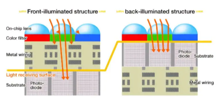
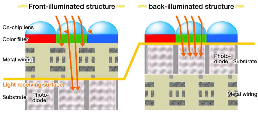
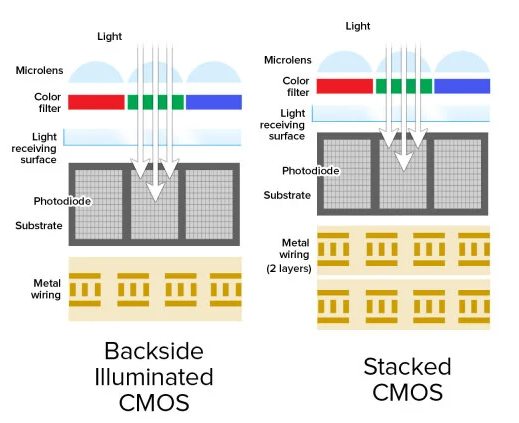
General CMOS pixels consist of several key components: on-chip lenses (microlenses), color filters (on-chip color filters), metal interconnects, photodiodes, and substrates.
Reference: https://en.wikipedia.org/wiki/Back-illuminated_sensor
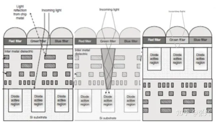
Traditionally, CMOS sensors have adopted a "front-illuminated" structure, as depicted on the left side of the illustration. When light penetrates the pixel, it traverses the on-chip lens and color filter before encountering the metal interconnect layer. Ultimately, the light is captured by the photodiode. However, metal, known for its opaqueness and reflectivity, poses a challenge. Light passing through the metal wiring layer is partially obstructed and reflected, resulting in a diminished light energy reaching the photodiode, often amounting to only 70% or less of the incident light. Moreover, this reflection can induce cross-talk with neighboring pixels, leading to color distortion. Notably, the prevalent metal used in the wiring layer of mid-to-low-end CMOS sensors is the relatively inexpensive aluminum (Al), which maintains a reflectivity of approximately 90% across the entire visible light spectrum (380-780nm).
In response to these limitations, the "back-illuminated" CMOS configuration emerged at an opportune moment. In this design, the positions of the metal wiring layer and the photodiode are reversed compared to the "front-illuminated" type. Consequently, light can directly reach the photodiode with minimal obstruction or interference. This results in significantly enhanced light utilization, making back-illuminated CMOS sensors exceptionally efficient in capturing incoming light. Consequently, they excel in low-light environments, offering superior image quality.
In summary, while traditional CMOS sensors have been hampered by the obstructive nature of metal interconnects, the advent of back-illuminated CMOS technology has addressed these shortcomings, paving the way for enhanced image quality, particularly in challenging lighting conditions.
CMOS vs BSI CMOS: Which is better
Let's delve deeper into analyzing the advantages and disadvantages of Frontside Illuminated (FSI) and Backside Illuminated (BSI) sensor technologies. But before we proceed, let's revisit their cross-sections. The dashed line delineates the location of the photodiode. This perspective offers a straightforward view of BSI's streamlined optical path, which translates to reduced consumption within the sensor.
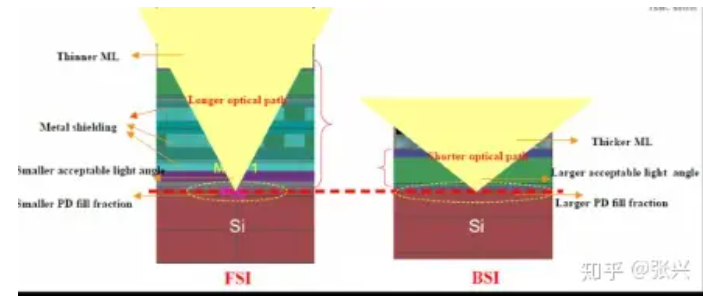
Advantages of FSI:
FSI adheres closely to semiconductor manufacturing processes. Light enters between the metal wiring on the front and converges onto the photodiode within the light-sensitive area. Even for larger pixels, FSI can still deliver satisfactory performance. Its relatively modest ratio of optical stack height to pixel area ensures a well-preserved photosensitive area. Moreover, FSI boasts a simple manufacturing process, yielding lower costs and higher efficiency compared to BSI. In terms of manufacturing process requirements, FSI generally presents lower demands than BSI.
Disadvantages of FSI:
However, as pixel sizes diminish, FSI encounters limitations such as reduced fill factor, elongated optical paths, and significant reflection and absorption losses within the metal wiring. These factors collectively impede sensor performance as pixel dimensions decrease.
Following the completion of the front-end process, BSI undergoes a distinctive procedure where the wafer is flipped, bonded, thinned, and subsequently outfitted with color filters and microlenses on the back.
Advantages of BSI:
BSI's hallmark advantage lies in its ability to segregate electrical components from light, enabling independent optimization of the light path and mitigating absorption and reflection by the FSI's metal wiring layer. Additionally, the optical stack within BSI pixels is substantially minimized, resulting in a larger fill factor, approaching nearly 100%. Consequently, BSI achieves higher Quantum Efficiency (QE).
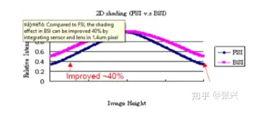
BSI's streamlined optical stack significantly reduces thickness, rendering it more amenable to incident angles. For instance, at a 1.4μm pixel size, the BSI structure can ameliorate lens shading by 40% compared to FSI.
Disadvantages of BSI:
Nevertheless, the BSI process is intricate and challenging. Early development stages and initial yield rates pose significant hurdles. Nonetheless, with ongoing advancements in semiconductor technology, BSI's viability has matured, with corresponding improvements in yield rates.
Moreover, the back-side-up orientation of BSI chips exposes the silicon body material near the photodiode to direct illumination. This can lead to crosstalk issues due to light diffusion into neighboring pixels or recombination at the back interface. Nonetheless, industry innovations are tackling these challenges by enhancing processing on the chip's rear.
As smartphones strive for slimmer profiles and smaller module heights, CMOS Image Sensor pixels are shrinking correspondingly. Meanwhile, technologies like Dual PDAF sensors and Quad pixel binning are gaining traction in mobile photography. This underscores the perpetual pursuit of superior image quality and underscores the industry's ongoing quest for enhanced photoelectric conversion efficiency.
Stacked Sensor vs BSI
Stacked sensor technology and Backside Illuminated (BSI) sensor technology are both significant advancements in the field of image sensor design, each offering unique benefits and applications.
Stacked Sensor
Stacked sensor technology involves the stacking of multiple semiconductor layers within a single sensor package. These layers can include the pixel layer (which contains the photodiodes), the logic layer (which processes the captured data), and additional layers for memory and other functionalities.
By stacking these layers vertically, stacked sensors can achieve higher pixel densities, faster readout speeds, and improved performance in various aspects such as dynamic range and low-light sensitivity.
The separate processing layer in stacked sensors enables more sophisticated signal processing and computational photography techniques, leading to enhanced image quality and innovative features like real-time HDR (High Dynamic Range) and high-speed continuous shooting.
Stacked sensor technology is commonly found in advanced digital cameras, smartphones, and other imaging devices where high performance and versatility are crucial.
Backside Illuminated (BSI) Sensor
BSI sensor technology addresses the challenge of light absorption and interference in traditional front-illuminated sensors by flipping the sensor architecture so that light enters through the backside of the sensor.
By placing the photodiodes closer to the surface of the sensor, BSI sensors can achieve higher light sensitivity and better performance, particularly in low-light conditions.
BSI sensors are especially beneficial for compact devices like smartphones, where space constraints limit the thickness of sensor layers and the amount of light that can reach the photodiodes.
The enhanced light sensitivity of BSI sensors also contributes to improved image quality, reduced noise, and better color accuracy, making them well-suited for a wide range of imaging applications.
Comparison
While both stacked sensor and BSI sensor technologies offer significant improvements over traditional sensor designs, they serve different purposes and excel in different areas.
Stacked sensors are prized for their versatility, high performance, and advanced computational capabilities, making them ideal for professional photography, videography, and demanding applications.
BSI sensors, on the other hand, prioritize compactness, low-light performance, and energy efficiency, making them well-suited for consumer electronics like smartphones and compact cameras where size and power consumption are critical factors.
|
Aspect |
Stacked Sensors |
BSI Sensors |
|
Purpose |
Versatility, high performance, advanced computational |
Compactness, low-light performance, energy efficiency |
|
capabilities |
||
|
Ideal Applications |
Professional photography, videography, demanding |
Consumer electronics like smartphones, compact cameras |
|
applications |
||
|
Performance |
High performance, fast readout speeds, improved dynamic |
Enhanced light sensitivity, better performance in low-light |
|
range, real-time HDR, high-speed continuous shooting |
conditions |
|
|
Size and Form Factor |
Typically larger and more complex due to stacked layers |
Compact and thin, suitable for small devices |
|
Power Consumption |
Consumption may be higher due to complex processing layers |
Generally lower due to efficient design and light |
|
and computational demands |
sensitivity |
|
|
Cost |
Generally higher due to advanced technology and features |
Cost-effective due to simpler design and manufacturing |
|
Market Segments |
Professional-grade cameras, high-end smartphones, |
Mass-market smartphones, compact cameras, entry-level |
|
specialized imaging applications |
digital cameras |
|
|
Customization and Innovation |
Offers opportunities for advanced features and |
Focuses on optimizing design for specific applications and |
|
computational photography techniques |
market demands |
BSI vs FSI Sensor
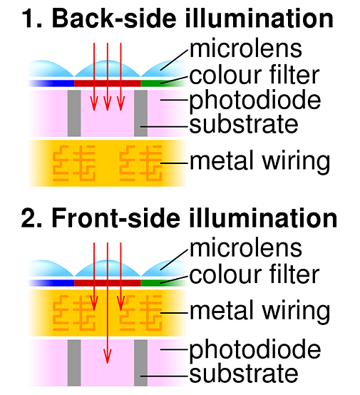
From the perspective of light incidence, CMOS sensors can be distinguished as "front-illuminated" and "back-illuminated". Literally, "front-illuminated" is akin to light shining directly onto the front of an object, while "back-illuminated" is akin to light shining onto the reverse side of an object.

As their names suggest, FSI sensors receive light through the front, while BSI sensors gather light from the back. This orientation corresponds to the front-end-of-line (FEOL) and back-end-of-line (BEOL) stages in semiconductor manufacturing. Essentially, it refers to the metal connection wiring within the semiconductor processing's latter stages.

During the evolution of FSI and BSI technologies, an intermediate concept emerged known as the wave-guided light guide structure. Building upon FSI principles, this structure optimizes the optical path to enhance light entry into the photosensitive area and bolster Quantum Efficiency (QE), which essentially evaluates the sensor's photoelectric conversion capabilities. The wave-guided approach entails infusing the metal with high refractive index material, enabling more effective light concentration within the light guide area between metal lines while minimizing light absorption and reflection by the metal wiring.
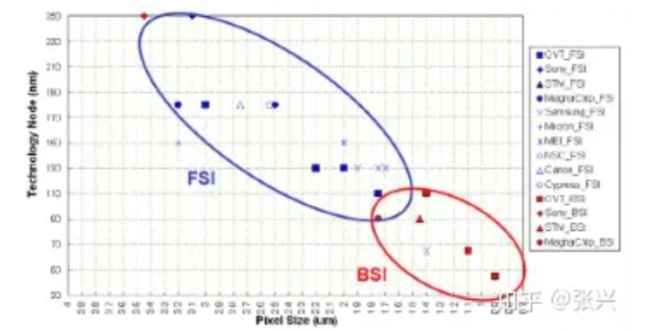
The graph below illustrates TSMC's summary of QE and Pixel trends for FSI and BSI sensors, showcasing the distinct advantages of the compact BSI structure. However, it's worth noting that this data reflects an earlier stage, with current QE values likely surpassing those depicted.
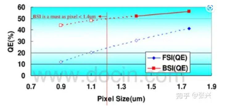
The industry's transition from FSI to BSI stems from shifts in sensor pixel sizes. Simply put, FSI suffices when pixel sizes are larger, obviating the need for BSI methods. The graph below illustrates the progression of FSI and BSI manufacturing processes relative to pixel size. As sensor pixel sizes shrink, the demand for performance and process precision escalates. Roughly speaking, the 2μm threshold serves as a dividing line; sensors below this mark predominantly adopt the BSI structure.
BSI CMOS vs CCD
BSI CMOS (Backside Illuminated Complementary Metal-Oxide-Semiconductor) and CCD (Charge-Coupled Device) represent two distinct technologies utilized in image sensors for digital imaging devices. Fundamentally, BSI CMOS sensors employ a CMOS technology where the photodiodes reside on the backside of the sensor, enabling light to directly reach them without hindrance. In contrast, CCD sensors operate on a different principle, relying on the movement of charge through a silicon substrate. This process involves photons entering the sensor, creating electron-hole pairs which are subsequently transported through the substrate for readout.
In terms of light sensitivity, BSI CMOS sensors are renowned for their heightened sensitivity, particularly in low-light conditions, owing to the unobstructed path of light to the photodiodes. Traditionally, CCD sensors held an edge in light sensitivity over traditional front-illuminated CMOS sensors. However, advancements in BSI CMOS technology have considerably narrowed this gap.
Another differentiating factor lies in readout speed. CMOS sensors, including BSI CMOS, typically offer faster readout speeds due to their parallel readout architecture. Conversely, CCD sensors historically exhibited slower readout speeds as charge transfer occurred serially through the sensor.
Moreover, power consumption varies between the two technologies. CMOS sensors, such as BSI CMOS, generally consume less power compared to CCD sensors, making them better suited for battery-powered devices like smartphones. CCD sensors, on the other hand, tend to consume more power due to their serial readout process and higher voltage requirements.
In terms of applications, BSI CMOS sensors have gained dominance in consumer electronics such as smartphones, digital cameras, and webcams due to their superior performance, lower power consumption, and faster readout speeds. Meanwhile, CCD sensors have retained their niche in specialized fields like astronomy, microscopy, and scientific imaging, where their unique characteristics are indispensable.
BSI CMOS vs APS-C
BSI CMOS (Backside Illuminated Complementary Metal-Oxide-Semiconductor) and APS-C (Advanced Photo System type-C) represent distinct aspects of digital imaging technology, each playing a significant role in the functionality and performance of modern cameras.
BSI CMOS technology is centered around the design of image sensors where photodiodes are positioned on the backside of the sensor. This configuration allows light to directly reach the photodiodes without obstruction, resulting in enhanced light sensitivity, particularly in low-light conditions. As a result, BSI CMOS sensors are widely utilized in digital cameras, smartphones, and various imaging devices where superior low-light performance and image quality are paramount.
In contrast, APS-C refers to a specific sensor size commonly employed in digital cameras. APS-C sensors are larger than those typically found in compact cameras and smartphones, but smaller than full-frame sensors. They strike a balance between image quality and portability, making them popular among enthusiasts and professionals alike. APS-C sensors are predominantly featured in interchangeable lens cameras such as DSLRs (Digital Single-Lens Reflex) and mirrorless cameras, offering photographers versatility in a relatively compact package.
In terms of light sensitivity and image quality, BSI CMOS sensors have a notable advantage due to their direct path of light to the photodiodes. This enables them to deliver excellent image quality with reduced noise, particularly in challenging lighting conditions. On the other hand, APS-C sensors offer good image quality with respectable dynamic range and color reproduction, although they may not match the low-light performance of BSI CMOS sensors.
Overall, both BSI CMOS and APS-C play crucial roles in modern photography and imaging technology. While BSI CMOS technology focuses on improving light sensitivity and image quality through sensor design, APS-C sensors provide photographers with a versatile and portable option for capturing high-quality images in various shooting scenarios.
BSI CMOS vs X-Trans
BSI CMOS (Backside Illuminated Complementary Metal-Oxide-Semiconductor) and X-Trans are two distinct technologies employed in digital imaging, each offering unique advantages and characteristics.
BSI CMOS technology revolves around the design of image sensors where photodiodes are located on the backside of the sensor. This configuration enables light to directly reach the photodiodes without obstruction, leading to enhanced light sensitivity, especially in low-light conditions. BSI CMOS sensors are widely utilized in digital cameras, smartphones, and various imaging devices, prioritizing superior low-light performance and image quality.
On the other hand, X-Trans is a proprietary sensor technology developed by Fujifilm, primarily utilized in their X-series mirrorless cameras. X-Trans sensors employ a unique color filter array (CFA) pattern that differs from the traditional Bayer array found in most digital cameras. This pattern is designed to reduce moiré and false color artifacts without the need for an optical low-pass filter, thereby enhancing image sharpness and detail rendition.
In terms of image quality, BSI CMOS sensors excel in low-light performance due to their direct path of light to the photodiodes, resulting in reduced noise and improved sensitivity. They are well-suited for capturing detailed images in challenging lighting conditions. On the other hand, X-Trans sensors offer excellent color reproduction and sharpness, thanks to their innovative CFA pattern. They provide photographers with enhanced image quality and reduced artifacts, particularly in high-resolution images.
Overall, BSI CMOS and X-Trans technologies cater to different aspects of digital imaging, with BSI CMOS prioritizing low-light performance and sensitivity, while X-Trans focuses on color accuracy, detail rendition, and reducing artifacts.
CMOS BSI vs ISOCELL
CMOS BSI (Backside Illuminated Complementary Metal-Oxide-Semiconductor) and ISOCELL are two different technologies utilized in the development of image sensors, each offering distinct advantages in digital imaging.
CMOS BSI technology involves positioning the photodiodes on the backside of the sensor, allowing light to directly reach them without obstruction. This design enhances light sensitivity, particularly in low-light conditions, and improves image quality by reducing noise and increasing dynamic range. CMOS BSI sensors are widely used in various imaging devices, including smartphones, digital cameras, and surveillance cameras, where superior low-light performance is essential.
On the other hand, ISOCELL is a proprietary sensor technology developed by Samsung Electronics. ISOCELL technology aims to improve image quality by minimizing crosstalk between pixels and enhancing light sensitivity. This is achieved by incorporating physical barriers between individual pixels, preventing light from bleeding into neighboring pixels and thereby improving color accuracy and sharpness. ISOCELL sensors are commonly found in Samsung smartphones and other mobile devices, delivering high-quality images with excellent color reproduction and detail.
In terms of performance, CMOS BSI sensors excel in low-light conditions due to their enhanced light sensitivity and reduced noise, making them ideal for capturing clear and detailed images in challenging lighting environments. On the other hand, ISOCELL sensors offer superior color accuracy and image sharpness, thanks to their innovative pixel isolation technology, providing users with high-quality images even in brightly lit scenarios.
BSI sensor vs Exmor RS CMOS Sensor
BSI sensors revolutionize light sensitivity by positioning photodiodes on the backside of the sensor, allowing light to directly reach them without obstacles. This design enhancement significantly improves image quality, particularly in low-light conditions, resulting in clearer images with reduced noise. Widely adopted in smartphones, surveillance cameras, and digital cameras, BSI sensors excel in scenarios where superior low-light performance is critical.
On the other hand, Exmor RS CMOS sensors, pioneered by Sony, introduce a stacked sensor design coupled with a back-illuminated structure. This innovation further enhances light sensitivity by minimizing the distance between photodiodes and the light-receiving surface. The result is exceptional performance in low-light environments, complemented by high-speed image capture capabilities. Commonly utilized in high-end digital cameras, smartphones, and professional video cameras, Exmor RS CMOS sensors deliver outstanding image quality with swift readout speeds and advanced signal processing capabilities.
While BSI sensors prioritize low-light sensitivity and noise reduction, Exmor RS CMOS sensors excel in high-speed performance and sophisticated signal processing.
BSI Sensor Cameras List
|
Type |
Brand and Model |
|
Smartphones |
Apple iPhone 12, iPhone 13 |
|
Samsung Galaxy S21, Galaxy Note 20 |
|
|
Google Pixel 6, Pixel 6 Pro |
|
|
Huawei P40, P50 |
|
|
Xiaomi Mi 11, Mi 11 Ultra |
|
|
Digital Cameras |
Sony Alpha A7S III, A7R IV |
|
Nikon Z6 II, Z7 II |
|
|
Canon EOS R6, EOS R5 |
|
|
Fujifilm X-T4, X-S10 |
|
|
Panasonic Lumix S1, S5 |
|
|
Action Cameras |
GoPro Hero 10 Black, Hero 9 Black |
|
DJI Action 2 |
|
|
Compact Cameras |
Sony Cyber-shot RX100 VII, RX100 VI |
|
Canon PowerShot G7 X Mark III, G5 X Mark II |
|
|
Panasonic Lumix LX100 II |
BSI CMOS Sensor Size
|
Sensor Size |
Description |
|
1/3.2-inch |
Found in entry-level smartphones and compact cameras. |
|
1/2.3-inch |
Used in mid-range smartphones, action cameras, and compact digital cameras. |
|
1/2-inch |
Commonly found in some higher-end smartphones and compact cameras. |
|
1/1.7-inch |
Seen in premium compact cameras and select high-end smartphones. |
|
APS-C |
Larger sensors used in mirrorless cameras and DSLRs, offering improved image quality and low-light performance. |
|
Full-frame |
The largest sensors found in professional-grade digital cameras, providing superior image quality, dynamic range, and low-light performance. |
Final Words
In conclusion, the comparison between CMOS and BSI sensors reveals a nuanced landscape where each technology excels in different areas. While CMOS sensors offer versatility, low power consumption, and potentially lower production costs, BSI sensors provide superior light sensitivity, reduced noise levels, and improved performance in low-light conditions.
Read More:
Size of Image Sensor: How Does Sensor Size Affect Image Quality
CCD vs CMOS: Difference Between CCD and CMOS Image Sensor
Throttle Position Sensor Diagram
Crankshaft Position Sensor Location
Temporary Fix for Crankshaft Position Sensor
How to Test Crankshaft Sensor with Multimeter
Where Is the Knock Sensor Located
How to Start a Car with a Bad Crankshaft Sensor
How to Start a Car with a Bad Crankshaft Sensor
How does the Oxygen Sensor OSS-2 Effectively Improve Vehicle Exhaust Pollution Emissions
Where are Radar Sensors on Mercedes
How Many Sensors Are In a Car【Types & Functions】
How to Delete O2 Sensors from ECM
How Many O2 Sensors Does a Car Have
4 Wire Oxygen Sensor Wiring Diagram
Can a Bad O2 Sensor Cause a Misfire
How to Reset a Mass Air Flow Sensor
- Size of Image Sensor: How Does Sensor Size Affect Image Quality
- CCD vs CMOS: Difference Between CCD and CMOS Image Sensor
- What is the Advantage of IGBT
- Difference Between IGBT and MOSFET (IGBT vs MOSFET)
- Global IGBT Shortage: Cause & Future Outlook
- Difference Between IGBT and Thyristor 【IGBT vs Thyristor】
- How to Test an IGBT Using A Multimeter
- IGBT Types: Understanding the Basics
Popular Manufacturers


Popular Car Brands