CMOS vs BSI Sensor
Feb 18, 2024 View: 4239
The debate between CMOS (Complementary Metal-Oxide-Semiconductor) and BSI (Backside-Illuminated) sensors has long been a topic of interest in the realm of digital imaging technology. Both sensor types have their own set of advantages and drawbacks, influencing their suitability for various applications. In this article, we will explore the key differences between CMOS and BSI sensors, examining their respective strengths and weaknesses, and discussing how these factors impact image quality, low-light performance, and overall camera functionality.
BSI CMOS vs CMOS
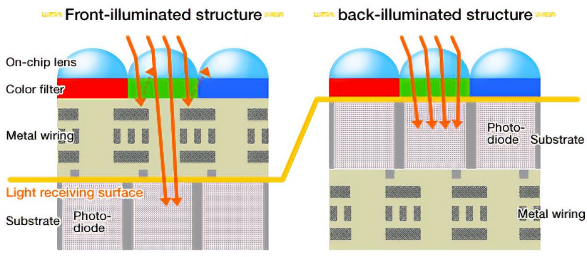
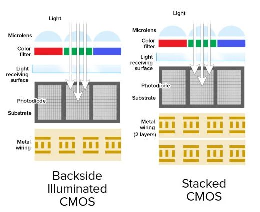
General CMOS pixels consist of several key components: on-chip lenses (microlenses), color filters (on-chip color filters), metal interconnects, photodiodes, and substrates.
Reference: https://en.wikipedia.org/wiki/Back-illuminated_sensor
Traditionally, CMOS sensors have adopted a "front-illuminated" structure, as depicted on the left side of the illustration. When light penetrates the pixel, it traverses the on-chip lens and color filter before encountering the metal interconnect layer. Ultimately, the light is captured by the photodiode. However, metal, known for its opaqueness and reflectivity, poses a challenge. Light passing through the metal wiring layer is partially obstructed and reflected, resulting in a diminished light energy reaching the photodiode, often amounting to only 70% or less of the incident light. Moreover, this reflection can induce cross-talk with neighboring pixels, leading to color distortion. Notably, the prevalent metal used in the wiring layer of mid-to-low-end CMOS sensors is the relatively inexpensive aluminum (Al), which maintains a reflectivity of approximately 90% across the entire visible light spectrum (380-780nm).
In response to these limitations, the "back-illuminated" CMOS configuration emerged at an opportune moment. In this design, the positions of the metal wiring layer and the photodiode are reversed compared to the "front-illuminated" type. Consequently, light can directly reach the photodiode with minimal obstruction or interference. This results in significantly enhanced light utilization, making back-illuminated CMOS sensors exceptionally efficient in capturing incoming light. Consequently, they excel in low-light environments, offering superior image quality.
In summary, while traditional CMOS sensors have been hampered by the obstructive nature of metal interconnects, the advent of back-illuminated CMOS technology has addressed these shortcomings, paving the way for enhanced image quality, particularly in challenging lighting conditions.
CMOS vs BSI CMOS: Which is better
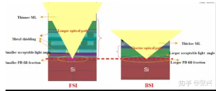
Let's delve deeper into analyzing the advantages and disadvantages of Frontside Illuminated (FSI) and Backside Illuminated (BSI) sensor technologies. But before we proceed, let's revisit their cross-sections. The dashed line delineates the location of the photodiode. This perspective offers a straightforward view of BSI's streamlined optical path, which translates to reduced consumption within the sensor.
Advantages of FSI:
FSI adheres closely to semiconductor manufacturing processes. Light enters between the metal wiring on the front and converges onto the photodiode within the light-sensitive area. Even for larger pixels, FSI can still deliver satisfactory performance. Its relatively modest ratio of optical stack height to pixel area ensures a well-preserved photosensitive area. Moreover, FSI boasts a simple manufacturing process, yielding lower costs and higher efficiency compared to BSI. In terms of manufacturing process requirements, FSI generally presents lower demands than BSI.
Disadvantages of FSI:
However, as pixel sizes diminish, FSI encounters limitations such as reduced fill factor, elongated optical paths, and significant reflection and absorption losses within the metal wiring. These factors collectively impede sensor performance as pixel dimensions decrease.
Following the completion of the front-end process, BSI undergoes a distinctive procedure where the wafer is flipped, bonded, thinned, and subsequently outfitted with color filters and microlenses on the back.
Advantages of BSI:
BSI's hallmark advantage lies in its ability to segregate electrical components from light, enabling independent optimization of the light path and mitigating absorption and reflection by the FSI's metal wiring layer. Additionally, the optical stack within BSI pixels is substantially minimized, resulting in a larger fill factor, approaching nearly 100%. Consequently, BSI achieves higher Quantum Efficiency (QE).
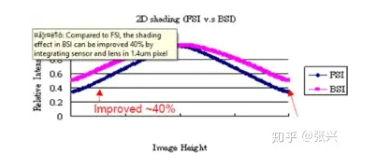
BSI's streamlined optical stack significantly reduces thickness, rendering it more amenable to incident angles. For instance, at a 1.4μm pixel size, the BSI structure can ameliorate lens shading by 40% compared to FSI.
Disadvantages of BSI:
Nevertheless, the BSI process is intricate and challenging. Early development stages and initial yield rates pose significant hurdles. Nonetheless, with ongoing advancements in semiconductor technology, BSI's viability has matured, with corresponding improvements in yield rates.
Moreover, the back-side-up orientation of BSI chips exposes the silicon body material near the photodiode to direct illumination. This can lead to crosstalk issues due to light diffusion into neighboring pixels or recombination at the back interface. Nonetheless, industry innovations are tackling these challenges by enhancing processing on the chip's rear.
As smartphones strive for slimmer profiles and smaller module heights, CMOS Image Sensor pixels are shrinking correspondingly. Meanwhile, technologies like Dual PDAF sensors and Quad pixel binning are gaining traction in mobile photography. This underscores the perpetual pursuit of superior image quality and underscores the industry's ongoing quest for enhanced photoelectric conversion efficiency.
Stacked Sensor vs BSI
Stacked sensor technology and Backside Illuminated (BSI) sensor technology are both significant advancements in the field of image sensor design, each offering unique benefits and applications.
Stacked Sensor
Stacked sensor technology involves the stacking of multiple semiconductor layers within a single sensor package. These layers can include the pixel layer (which contains the photodiodes), the logic layer (which processes the captured data), and additional layers for memory and other functionalities.
By stacking these layers vertically, stacked sensors can achieve higher pixel densities, faster readout speeds, and improved performance in various aspects such as dynamic range and low-light sensitivity.
The separate processing layer in stacked sensors enables more sophisticated signal processing and computational photography techniques, leading to enhanced image quality and innovative features like real-time HDR (High Dynamic Range) and high-speed continuous shooting.
Stacked sensor technology is commonly found in advanced digital cameras, smartphones, and other imaging devices where high performance and versatility are crucial.
Backside Illuminated (BSI) Sensor
BSI sensor technology addresses the challenge of light absorption and interference in traditional front-illuminated sensors by flipping the sensor architecture so that light enters through the backside of the sensor.
By placing the photodiodes closer to the surface of the sensor, BSI sensors can achieve higher light sensitivity and better performance, particularly in low-light conditions.
BSI sensors are especially beneficial for compact devices like smartphones, where space constraints limit the thickness of sensor layers and the amount of light that can reach the photodiodes.
The enhanced light sensitivity of BSI sensors also contributes to improved image quality, reduced noise, and better color accuracy, making them well-suited for a wide range of imaging applications.
Comparison
While both stacked sensor and BSI sensor technologies offer significant improvements over traditional sensor designs, they serve different purposes and excel in different areas.
Stacked sensors are prized for their versatility, high performance, and advanced computational capabilities, making them ideal for professional photography, videography, and demanding applications.
BSI sensors, on the other hand, prioritize compactness, low-light performance, and energy efficiency, making them well-suited for consumer electronics like smartphones and compact cameras where size and power consumption are critical factors.
|
Aspect |
Stacked Sensors |
BSI Sensors |
|
Purpose |
Versatility, high performance, advanced computational |
Compactness, low-light performance, energy efficiency |
|
capabilities |
||
|
Ideal Applications |
Professional photography, videography, demanding |
Consumer electronics like smartphones, compact cameras |
|
applications |
||
|
Performance |
High performance, fast readout speeds, improved dynamic |
Enhanced light sensitivity, better performance in low-light |
|
range, real-time HDR, high-speed continuous shooting |
conditions |
|
|
Size and Form Factor |
Typically larger and more complex due to stacked layers |
Compact and thin, suitable for small devices |
|
Power Consumption |
Consumption may be higher due to complex processing layers |
Generally lower due to efficient design and light |
|
and computational demands |
sensitivity |
|
|
Cost |
Generally higher due to advanced technology and features |
Cost-effective due to simpler design and manufacturing |
|
Market Segments |
Professional-grade cameras, high-end smartphones, |
Mass-market smartphones, compact cameras, entry-level |
|
specialized imaging applications |
digital cameras |
|
|
Customization and Innovation |
Offers opportunities for advanced features and |
Focuses on optimizing design for specific applications and |
|
computational photography techniques |
market demands |
BSI vs FSI Sensor
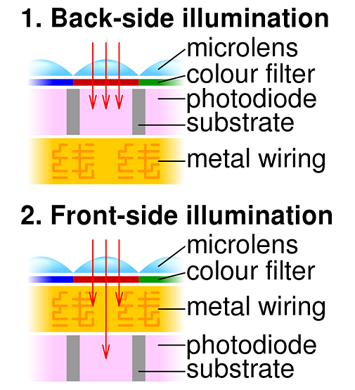
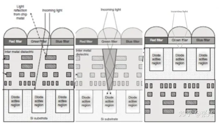
From the perspective of light incidence, CMOS sensors can be distinguished as "front-illuminated" and "back-illuminated". Literally, "front-illuminated" is akin to light shining directly onto the front of an object, while "back-illuminated" is akin to light shining onto the reverse side of an object.

As their names suggest, FSI sensors receive light through the front, while BSI sensors gather light from the back. This orientation corresponds to the front-end-of-line (FEOL) and back-end-of-line (BEOL) stages in semiconductor manufacturing. Essentially, it refers to the metal connection wiring within the semiconductor processing's latter stages.

During the evolution of FSI and BSI technologies, an intermediate concept emerged known as the wave-guided light guide structure. Building upon FSI principles, this structure optimizes the optical path to enhance light entry into the photosensitive area and bolster Quantum Efficiency (QE), which essentially evaluates the sensor's photoelectric conversion capabilities. The wave-guided approach entails infusing the metal with high refractive index material, enabling more effective light concentration within the light guide area between metal lines while minimizing light absorption and reflection by the metal wiring.
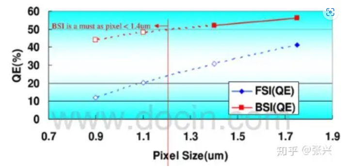
The graph below illustrates TSMC's summary of QE and Pixel trends for FSI and BSI sensors, showcasing the distinct advantages of the compact BSI structure. However, it's worth noting that this data reflects an earlier stage, with current QE values likely surpassing those depicted.
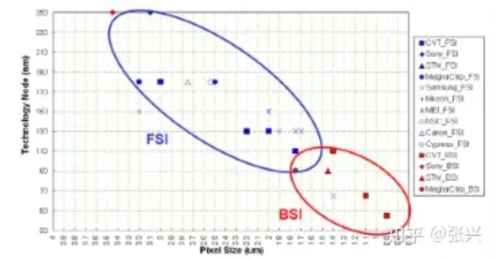
The industry's transition from FSI to BSI stems from shifts in sensor pixel sizes. Simply put, FSI suffices when pixel sizes are larger, obviating the need for BSI methods. The graph below illustrates the progression of FSI and BSI manufacturing processes relative to pixel size. As sensor pixel sizes shrink, the demand for performance and process precision escalates. Roughly speaking, the 2μm threshold serves as a dividing line; sensors below this mark predominantly adopt the BSI structure.
BSI CMOS vs CCD
BSI CMOS (Backside Illuminated Complementary Metal-Oxide-Semiconductor) and CCD (Charge-Coupled Device) represent two distinct technologies utilized in image sensors for digital imaging devices. Fundamentally, BSI CMOS sensors employ a CMOS technology where the photodiodes reside on the backside of the sensor, enabling light to directly reach them without hindrance. In contrast, CCD sensors operate on a different principle, relying on the movement of charge through a silicon substrate. This process involves photons entering the sensor, creating electron-hole pairs which are subsequently transported through the substrate for readout.
In terms of light sensitivity, BSI CMOS sensors are renowned for their heightened sensitivity, particularly in low-light conditions, owing to the unobstructed path of light to the photodiodes. Traditionally, CCD sensors held an edge in light sensitivity over traditional front-illuminated CMOS sensors. However, advancements in BSI CMOS technology have considerably narrowed this gap.
Another differentiating factor lies in readout speed. CMOS sensors, including BSI CMOS, typically offer faster readout speeds due to their parallel readout architecture. Conversely, CCD sensors historically exhibited slower readout speeds as charge transfer occurred serially through the sensor.
Moreover, power consumption varies between the two technologies. CMOS sensors, such as BSI CMOS, generally consume less power compared to CCD sensors, making them better suited for battery-powered devices like smartphones. CCD sensors, on the other hand, tend to consume more power due to their serial readout process and higher voltage requirements.
In terms of applications, BSI CMOS sensors have gained dominance in consumer electronics such as smartphones, digital cameras, and webcams due to their superior performance, lower power consumption, and faster readout speeds. Meanwhile, CCD sensors have retained their niche in specialized fields like astronomy, microscopy, and scientific imaging, where their unique characteristics are indispensable.
BSI CMOS vs APS-C
BSI CMOS (Backside Illuminated Complementary Metal-Oxide-Semiconductor) and APS-C (Advanced Photo System type-C) represent distinct aspects of digital imaging technology, each playing a significant role in the functionality and performance of modern cameras.
BSI CMOS technology is centered around the design of image sensors where photodiodes are positioned on the backside of the sensor. This configuration allows light to directly reach the photodiodes without obstruction, resulting in enhanced light sensitivity, particularly in low-light conditions. As a result, BSI CMOS sensors are widely utilized in digital cameras, smartphones, and various imaging devices where superior low-light performance and image quality are paramount.
In contrast, APS-C refers to a specific sensor size commonly employed in digital cameras. APS-C sensors are larger than those typically found in compact cameras and smartphones, but smaller than full-frame sensors. They strike a balance between image quality and portability, making them popular among enthusiasts and professionals alike. APS-C sensors are predominantly featured in interchangeable lens cameras such as DSLRs (Digital Single-Lens Reflex) and mirrorless cameras, offering photographers versatility in a relatively compact package.
In terms of light sensitivity and image quality, BSI CMOS sensors have a notable advantage due to their direct path of light to the photodiodes. This enables them to deliver excellent image quality with reduced noise, particularly in challenging lighting conditions. On the other hand, APS-C sensors offer good image quality with respectable dynamic range and color reproduction, although they may not match the low-light performance of BSI CMOS sensors.
Overall, both BSI CMOS and APS-C play crucial roles in modern photography and imaging technology. While BSI CMOS technology focuses on improving light sensitivity and image quality through sensor design, APS-C sensors provide photographers with a versatile and portable option for capturing high-quality images in various shooting scenarios.
BSI CMOS vs X-Trans
BSI CMOS (Backside Illuminated Complementary Metal-Oxide-Semiconductor) and X-Trans are two distinct technologies employed in digital imaging, each offering unique advantages and characteristics.
BSI CMOS technology revolves around the design of image sensors where photodiodes are located on the backside of the sensor. This configuration enables light to directly reach the photodiodes without obstruction, leading to enhanced light sensitivity, especially in low-light conditions. BSI CMOS sensors are widely utilized in digital cameras, smartphones, and various imaging devices, prioritizing superior low-light performance and image quality.
On the other hand, X-Trans is a proprietary sensor technology developed by Fujifilm, primarily utilized in their X-series mirrorless cameras. X-Trans sensors employ a unique color filter array (CFA) pattern that differs from the traditional Bayer array found in most digital cameras. This pattern is designed to reduce moiré and false color artifacts without the need for an optical low-pass filter, thereby enhancing image sharpness and detail rendition.
In terms of image quality, BSI CMOS sensors excel in low-light performance due to their direct path of light to the photodiodes, resulting in reduced noise and improved sensitivity. They are well-suited for capturing detailed images in challenging lighting conditions. On the other hand, X-Trans sensors offer excellent color reproduction and sharpness, thanks to their innovative CFA pattern. They provide photographers with enhanced image quality and reduced artifacts, particularly in high-resolution images.
Overall, BSI CMOS and X-Trans technologies cater to different aspects of digital imaging, with BSI CMOS prioritizing low-light performance and sensitivity, while X-Trans focuses on color accuracy, detail rendition, and reducing artifacts.
CMOS BSI vs ISOCELL
CMOS BSI (Backside Illuminated Complementary Metal-Oxide-Semiconductor) and ISOCELL are two different technologies utilized in the development of image sensors, each offering distinct advantages in digital imaging.
CMOS BSI technology involves positioning the photodiodes on the backside of the sensor, allowing light to directly reach them without obstruction. This design enhances light sensitivity, particularly in low-light conditions, and improves image quality by reducing noise and increasing dynamic range. CMOS BSI sensors are widely used in various imaging devices, including smartphones, digital cameras, and surveillance cameras, where superior low-light performance is essential.
On the other hand, ISOCELL is a proprietary sensor technology developed by Samsung Electronics. ISOCELL technology aims to improve image quality by minimizing crosstalk between pixels and enhancing light sensitivity. This is achieved by incorporating physical barriers between individual pixels, preventing light from bleeding into neighboring pixels and thereby improving color accuracy and sharpness. ISOCELL sensors are commonly found in Samsung smartphones and other mobile devices, delivering high-quality images with excellent color reproduction and detail.
In terms of performance, CMOS BSI sensors excel in low-light conditions due to their enhanced light sensitivity and reduced noise, making them ideal for capturing clear and detailed images in challenging lighting environments. On the other hand, ISOCELL sensors offer superior color accuracy and image sharpness, thanks to their innovative pixel isolation technology, providing users with high-quality images even in brightly lit scenarios.
BSI sensor vs Exmor RS CMOS Sensor
BSI sensors revolutionize light sensitivity by positioning photodiodes on the backside of the sensor, allowing light to directly reach them without obstacles. This design enhancement significantly improves image quality, particularly in low-light conditions, resulting in clearer images with reduced noise. Widely adopted in smartphones, surveillance cameras, and digital cameras, BSI sensors excel in scenarios where superior low-light performance is critical.
On the other hand, Exmor RS CMOS sensors, pioneered by Sony, introduce a stacked sensor design coupled with a back-illuminated structure. This innovation further enhances light sensitivity by minimizing the distance between photodiodes and the light-receiving surface. The result is exceptional performance in low-light environments, complemented by high-speed image capture capabilities. Commonly utilized in high-end digital cameras, smartphones, and professional video cameras, Exmor RS CMOS sensors deliver outstanding image quality with swift readout speeds and advanced signal processing capabilities.
While BSI sensors prioritize low-light sensitivity and noise reduction, Exmor RS CMOS sensors excel in high-speed performance and sophisticated signal processing.
BSI Sensor Cameras List
|
Type |
Brand and Model |
|
Smartphones |
Apple iPhone 12, iPhone 13 |
|
Samsung Galaxy S21, Galaxy Note 20 |
|
|
Google Pixel 6, Pixel 6 Pro |
|
|
Huawei P40, P50 |
|
|
Xiaomi Mi 11, Mi 11 Ultra |
|
|
Digital Cameras |
Sony Alpha A7S III, A7R IV |
|
Nikon Z6 II, Z7 II |
|
|
Canon EOS R6, EOS R5 |
|
|
Fujifilm X-T4, X-S10 |
|
|
Panasonic Lumix S1, S5 |
|
|
Action Cameras |
GoPro Hero 10 Black, Hero 9 Black |
|
DJI Action 2 |
|
|
Compact Cameras |
Sony Cyber-shot RX100 VII, RX100 VI |
|
Canon PowerShot G7 X Mark III, G5 X Mark II |
|
|
Panasonic Lumix LX100 II |
BSI CMOS Sensor Size
|
Sensor Size |
Description |
|
1/3.2-inch |
Found in entry-level smartphones and compact cameras. |
|
1/2.3-inch |
Used in mid-range smartphones, action cameras, and compact digital cameras. |
|
1/2-inch |
Commonly found in some higher-end smartphones and compact cameras. |
|
1/1.7-inch |
Seen in premium compact cameras and select high-end smartphones. |
|
APS-C |
Larger sensors used in mirrorless cameras and DSLRs, offering improved image quality and low-light performance. |
|
Full-frame |
The largest sensors found in professional-grade digital cameras, providing superior image quality, dynamic range, and low-light performance. |
Final Words
In conclusion, the comparison between CMOS and BSI sensors reveals a nuanced landscape where each technology excels in different areas. While CMOS sensors offer versatility, low power consumption, and potentially lower production costs, BSI sensors provide superior light sensitivity, reduced noise levels, and improved performance in low-light conditions.
Read More:
Size of Image Sensor: How Does Sensor Size Affect Image Quality
CCD vs CMOS: Difference Between CCD and CMOS Image Sensor
Throttle Position Sensor Diagram
Crankshaft Position Sensor Location
Temporary Fix for Crankshaft Position Sensor
How to Test Crankshaft Sensor with Multimeter
Where Is the Knock Sensor Located
How to Start a Car with a Bad Crankshaft Sensor
How to Start a Car with a Bad Crankshaft Sensor
How does the Oxygen Sensor OSS-2 Effectively Improve Vehicle Exhaust Pollution Emissions
Where are Radar Sensors on Mercedes
How Many Sensors Are In a Car【Types & Functions】
How to Delete O2 Sensors from ECM
How Many O2 Sensors Does a Car Have
4 Wire Oxygen Sensor Wiring Diagram
Can a Bad O2 Sensor Cause a Misfire
How to Reset a Mass Air Flow Sensor
Can I Use a Downstream Oxygen Sensor for Upstream
Previous: Size of Image Sensor: How Does Sensor Size Affect Image Quality
 FAQ
FAQ
- Is A7 IV a BSI?
- Yes, the Sony A7 IV (A7IV) features a backside-illuminated (BSI) CMOS sensor with a resolution of 33 megapixels.
- Is the Nikon Z9 a BSI sensor?
- Yes, the Nikon Z9 features a backside-illuminated (BSI) sensor with a resolution of 45 megapixels.
- Is Full-Frame better than APS-C?
- Full-frame cameras generally have better image quality and shallower depth of field, making them suitable for photography scenarios that require high quality and background blur. However, APS-C cameras are lighter in size and weight and more affordable, making them suitable for photographers who require portability and economy. Full-frame cameras may be more suitable for professional applications, such as commercial photography or photojournalism, while APS-C cameras are suitable for a variety of photography types.
- Is the Z50 sensor a BSI?
- Yes, the Nikon Z50 features a BSI (Backside Illuminated) CMOS sensor. This sensor design allows for improved light sensitivity and enhanced performance, particularly in low-light conditions. The 20.9MP BSI CMOS sensor used in the Nikon Z50 is derived from the D500's sensor technology, offering high-resolution image capture with excellent image quality. Additionally, the on-sensor phase detection enables fast and accurate autofocus, contributing to the camera's overall performance.
- Is CMOS mirrorless?
- Yes, CMOS (Complementary Metal-Oxide-Semiconductor) sensors are commonly used in mirrorless cameras. Mirrorless cameras utilize digital imaging sensors, such as CMOS sensors, to capture light and create images without the need for a mirror mechanism like those found in DSLR (Digital Single-Lens Reflex) cameras. CMOS sensors are preferred in mirrorless cameras for their high-speed performance, low power consumption, and ability to capture high-quality images. They are available in various sensor sizes, including full-frame, APS-C, and micro four-thirds, each offering different advantages in terms of image quality, low-light performance, and depth of field control.
- What is a BSI sensor?
- A Backside Illuminated (BSI) sensor, also known as a back-illuminated sensor, is a type of imaging sensor used in digital cameras. It features a unique layout that differs from traditional sensors, allowing for more efficient collection of light at the pixel level. In a BSI sensor, the photodiodes, which are responsible for capturing light and converting it into electrical signals, are positioned on the backside of the sensor. This arrangement enables light to directly reach the photodiodes without being obstructed by layers of circuitry and wiring, as is the case with front-illuminated sensors. By relocating the photodiodes to the backside of the sensor, BSI technology maximizes the sensor's light-gathering capability, resulting in improved sensitivity, especially in low-light conditions. This enhancement in light sensitivity translates to better image quality, reduced noise, and enhanced dynamic range in photographs.
Latest Blogs
Popular Manufacturers