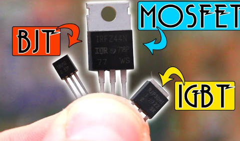
Difference Between BJT, MOSFET and IGBT: BJT vs MOSFET vs IGBT
Oct 24, 2023 View: 7393
Introduction
Choosing the most suitable power transistor for your electronic circuits is a critical decision that every designer must make. With a wide range of options available, including IGBTs, BJTs, and MOSFETs, the decision you make can have a profound impact on the overall performance of your circuit. As a designer, you frequently find yourself in the quandary of whether to opt for BJTs or MOSFETs in your power stage or, alternatively, consider the advantages of IGBTs. The questions at hand are substantial: Will these components be a good fit for your specific application? Will they enhance the overall design? In this comprehensive exploration, we will thoroughly examine the key distinctions between BJT, MOSFET, and IGBT, enabling you to make well-informed decisions that align with the specific requirements of your project.
Catalog:
What is BJT
What is MOSFET
What is IGBT
Difference Between BJT, MOSFET and IGBT
IGBT vs MOSFET
IGBT vs BJT: Difference Between IGBT and BJT
BJT Transistor vs MOSFET: Difference Between BJT and MOSFET
Advantages of IGBT Over MOSFET and BJT
Final Words
FAQ
What is BJT
A bipolar junction transistor (BJT) is a fundamental semiconductor device featuring three terminals and two p-n junctions. It operates as an amplifier or signal magnifier, making it a cornerstone of modern electronics. Being a current-controlled device, the BJT's behavior is primarily determined by the current flowing through its terminals.
The three essential terminals of a BJT are the base, collector, and emitter. When a small-amplitude signal is applied to the base terminal, the BJT demonstrates its amplification prowess by delivering an amplified version of that signal at the collector terminal. This amplification capability is a fundamental aspect of BJT's functionality, and it plays a vital role in various applications, including signal processing, amplification, and signal modulation. It's worth noting that for the BJT to carry out this signal amplification, it relies on an external source of DC (Direct Current) power supply. There are two primary types:
-
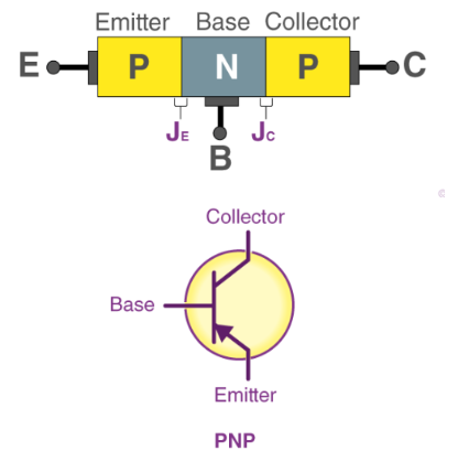
PNP BJT
In a PNP BJT, the core structure consists of an n-type semiconductor situated between two p-type semiconductors. The p-type semiconductors serve as the emitter and collector, while the n-type semiconductor functions as the base. This configuration allows for the flow of current to enter the transistor through the emitter, maintaining a forward-biased emitter-base junction and a reverse-biased collector-base junction.
-
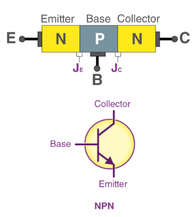
NPN BJT
The NPN BJT is characterized by a p-type semiconductor nestled between two n-type semiconductors. In this arrangement, the n-type semiconductors act as the emitter and collector, with the p-type semiconductor serving as the base. Current entering the emitter, base, and collector follows the positive sign convention, while the current exiting the transistor adheres to the negative sign convention.
What is MOSFET
MOSFET Structure
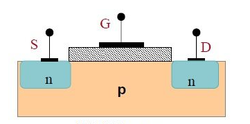
MOSFET is an acronym formed from the combination of "Metal Oxide Semiconductor" (MOS) and "Field-Effect Transistor" (FET). Its operational principle involves applying voltage to the gate, typically made of a metal layer (M, often aluminum), which is separated from the source by an insulating oxide layer (O, commonly silicon dioxide, SiO2). This voltage application generates an electric field within the semiconductor (S), thereby controlling the state of the electrical conduction channel. The presence of silicon dioxide insulation between the gate and both the source and drain regions has led to MOSFETs being referred to as "insulated-gate" field-effect transistors.
It's important to note that field-effect transistors come in two distinct structures: junction-type and insulated-gate-type. Field-effect transistors are semiconductor devices that rely on the electric field effect within their input circuit to control the current in their output circuit. They are often referred to as unipolar transistors because they primarily rely on majority carriers within the semiconductor to facilitate conduction.
Junction-type power field-effect transistors are commonly known as Static Induction Transistors (SIT). These devices are characterized by the use of gate voltage to control the current between the source and drain. They offer simple drive circuitry, low power requirements, rapid switching speeds, high operating frequencies, and excellent thermal stability. However, they have limited current-carrying capacities and voltage tolerance, typically suitable for power electronic applications up to 10 kilowatts.
On the other hand, MOSFET power field-effect transistors are primarily used for switching and driving applications, operating predominantly in a switching mode. Their voltage tolerance ranges from a few tens of volts to over a thousand volts, with current handling capabilities ranging from a few amperes to several tens of amperes. The majority of power MOSFETs belong to the enhanced-type category, known for their exceptional switching characteristics.
MOSFETs can be categorized based on the type of conduction channel as P-channel and N-channel. Furthermore, they can be classified according to the magnitude of the gate voltage as depletion-type and enhancement-type. In the depletion-type, a conductive channel between the drain and source still exists when the gate voltage is zero. Conversely, in the enhancement-type, for N (P)-channel devices, a conductive channel only forms when the gate voltage is greater than (less than) zero. Power MOSFETs primarily fall under the category of N-channel enhancement-type.
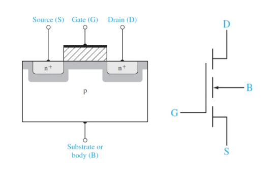
N-channel enhancement-type MOSFET Structure and Electrical Symbols
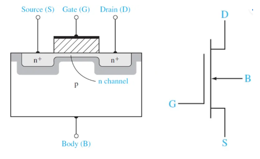
N-channel depletion-type MOSFET Structure and Electrical Symbols
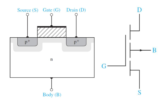
P-channel enhancement-type MOSFET Structure and Electrical Symbols
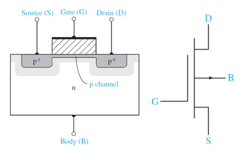
P-channel depletion-type MOSFET Structure and Electrical Symbols
What is IGBT
The Insulated Gate Bipolar Transistor (IGBT) is a fully controllable voltage-driven power semiconductor device that combines the characteristics of a bipolar junction transistor (BJT) and an insulated gate field-effect transistor (MOSFET). It finds its primary applications in fields demanding highly intricate control, such as automotive electronics, inverters, and railway transportation.
IGBT can be understood as a "non-conducting when off" switch, with the capability to invert direct current voltage into variable-frequency alternating current. This feature positions it as a vital component in variable-frequency inversion and other inversion circuits, earning it the moniker of the "CPU of power electronics devices."
IGBT has three terminals, including the collector, emitter, and gate, all of which are coated with a layer of metal. However, the gate terminal has an additional layer of silicon dioxide on the metal material.
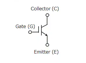
The structure of the IGBT is a four-layer semiconductor device. This four-layer structure is achieved by combining PNP and NPN transistors, forming a PNPN configuration.
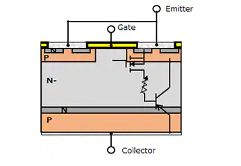
As shown in the figure above, the layer closest to the collector region is the (p+) substrate, known as the injection region. Above it lies the N-drift region, consisting of the N layer. The injection region serves to channel a significant portion of the charge carriers (hole current) from the (p+) layer into the N-layer.
Difference Between BJT, MOSFET and IGBT
|
Aspect |
IGBT |
BJT |
MOSFET |
|
Full Form |
Insulated Gate Bipolar Transistor |
Bipolar Junction Transistor |
Metal-Oxide-Semiconductor Field-Effect Transistor |
|
Symbol |
|
|
|
|
Terminals |
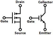
Collector, Emitter, Gate |
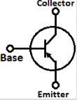
Collector, Emitter, Base |
Drain, Source, Gate |
|
Type of Device |
Combines characteristics of BJT and MOSFET, voltage-controlled bipolar device |
Bipolar transistor, current-controlled |
Field-effect transistor, voltage-controlled |
|
Gate or Base Control |
Gate control |
Base control |
Gate control |
|
Voltage and Current Ratings |
Suitable for high voltage and high current applications |
Moderate voltage and current ratings |
Moderate to high voltage, moderate current ratings |
|
Switching Frequency |
Moderate switching frequency |
Low switching frequency |
High switching frequency |
|
Gate Drive |
Requires higher gate drive voltage |
Requires current drive to the base |
Requires voltage drive to the gate |
|
Snubber Circuit |
Often requires snubber circuits for switching noise |
Less prone to switching noise; snubbers are less common |
May require snubbers, but less often than IGBT |
|
Voltage Blocking Capability |
High voltage blocking capability |
Moderate voltage blocking capability |
Moderate voltage blocking capability |
|
Temperature Coefficient |
Less sensitive to temperature variations |
Moderate sensitivity to temperature |
Moderate sensitivity to temperature |
|
Paralleling |
Suitable for parallel operation |
Challenging to parallel due to current sharing issues |
Can be paralleled with care |
|
Applications |
Used in high-power applications, such as inverters, motor drives, and power electronics |
Commonly found in low to medium power amplification and switching circuits |
Used in a wide range of applications, including power amplification, low to medium power switching, and in integrated circuits |
IGBT vs MOSFET
|
Parameter |
IGBT |
MOSFET |
|
Full Form |
Insulated Gate Bipolar Transistor |
Metal Oxide Semiconductor Field Effect Transistor |
|
Definition |
Three-terminal semiconductor switch used for signal switching and amplification |
Four-terminal semiconductor switch used for switching and amplification |
|
Terminals |
Emitter (E), Gate (G), Collector (C) |
Source (S), Gate (G), Drain (D) |
|
PN junction |
Has PN junctions in its construction |
Does not have any PN junctions |
|
Suitability |
Suitable for medium to high current control |
Suitable for low to medium current control |
|
Voltage and power handling |
Handles very high voltage and power |
Handles low to medium voltage and power |
|
Operating frequency |
Suitable for low frequencies (up to a few kHz) |
Suitable for very high frequencies (in the MHz range) |
|
Forward voltage drop |
Produces low forward voltage drop when conducting current |
Produces higher forward voltage drop |
|
Turn OFF time |
Longer turn-off time |
Shorter turn-off time |
|
Switching speed |
Relatively slower switching speed |
Very fast switching speed |
|
Transient voltage & current handling |
Can handle transient voltage and current |
Sensitive to transients and may be disrupted by them |
|
Saturation voltage |
Low saturation voltage |
High saturation voltage |
|
Cost |
Costlier |
Relatively low cost |
|
Applications |
high-power AC applications like inverter circuits |
low-power DC applications such as power supplies |
Read more: Difference Between IGBT and MOSFET (IGBT vs MOSFET)
IGBT vs BJT: Difference Between IGBT and BJT
|
Parameter |
BJT |
IGBT |
|
Full form |
Bipolar Junction Transistor |
Insulated Gate Bipolar Transistor |
|
Definition |
3-Terminal, Switching, Amplification |
3-Terminal, Power Electronics |
|
Terminals |
Emitter, Base, Collector |
Emitter, Collector, Gate |
|
Control quantity |
Current |
Voltage |
|
Control terminal |
Base |
Gate |
|
Drive circuit |
Complex |
Simple |
|
Switching speed |
Slow |
Fast |
|
Switching time |
10μs |
0.5μs |
|
Drive power |
High |
Low |
|
Switching power losses |
High |
Low |
|
Switching frequency rating |
20kHz |
160kHz |
|
Input impedance |
Low |
High |
|
Safe operating area (S.O.A.) |
Narrow |
Wide |
|
Power handling capacity |
Lower |
Higher |
|
ON-state resistance temp coeff |
Negative |
Positive |
|
Applications |
Low-power, Amplification |
Inverters, High-power |
BJT Transistor vs MOSFET: Difference Between BJT and MOSFET
|
Difference |
MOSFET |
BJT |
|
Type of Device |
Voltage controlled metal-oxide semiconductor |
Current controlled bipolar junction transistor |
|
Number of Terminals |
Three terminals: source, drain, gate |
Three terminals: base, emitter, collector |
|
Application Suitability |
Ideal for high-power applications |
More common in low-current applications |
|
Control Parameter |
Depends on the voltage at the oxide-insulated gate electrode |
Depends on the current at its base terminal |
|
Complexity of Structure |
Inherently more complex structure |
Simpler structure |
Advantages of IGBT Over MOSFET and BJT
In industries, there is a demand for converters that can operate across a wide voltage and power range. Traditional power devices, such as Bipolar Junction Transistors (BJTs) and Metal Oxide Semiconductor Field Effect Transistors (MOSFETs), have limitations in meeting these requirements.
BJTs offer lower ON state conduction losses and can handle higher voltages, but they have longer switching rates and are susceptible to secondary breakdown due to local hotspots.
MOSFETs have faster switching rates but suffer from higher ON state losses and cannot handle high voltages.
To combine the advantages of both BJT and MOSFET, the Insulated Gate Bipolar Transistor (IGBT) was introduced. It's a three-terminal device that offers low ON-state conduction losses and high switching speeds, up to 30kHz. IGBT's three terminals (Gate, Collector, and Emitter) are derived from BJT and MOSFET.
Although IGBT has several advantages, it has a significant drawback, known as the latching problem, where the device may not turn off even when the gate voltage is below the threshold. This necessitates external circuitry for turning off the IGBT, adding complexity to circuit design.
Final Words
In general, BJT, MOSFET and IGBT are three different types of semiconductor switching devices, each with unique working principles and characteristics. BJTs are suitable for low power and low frequency applications, MOSFETs excel in high frequency and high speed switching applications, and IGBTs are mainly used in high voltage and high current applications. These devices differ in switching speed, power consumption, driver complexity, and thermal management, so selection requires trade-offs based on the needs of the specific application. Circuit design, thermal and driver circuit considerations are critical to ensuring performance and reliability.
Read More:
IGCT vs. IGBT: What Are the Difference
IGBT vs GTO: Difference Between IGBT and GTO
IGBT Structure, Characteristics and Working Principle
Application of IGBT and IGBT Application Examples
IGBT Symbol Diagram, Characteristics, Circuit
Global IGBT Shortage: Cause & Future Outlook
IGBT Rectifier: All You Want to Know
IGBT Types: Understanding the Basics
How to Test an IGBT with A Multimeter
Difference Between IGBT and MOSFET (IGBT vs MOSFET)
What is the Advantage of IGBT
Difference Between IGBT and Thyristor
 FAQ
FAQ
- Does MOSFET switch faster than BJT?
- In most cases, MOSFETs hold the upper hand when it comes to switching speed. The key distinction lies in the fact that BJTs are current-controlled devices, meaning their switching speed heavily relies on the driver's strength. Conversely, MOSFETs, being voltage-controlled and simpler in nature, tend to exhibit much faster gate switching speeds.
- Is a BJT unidirectional or bidirectional?
- Unidirectional device.
- Which is faster, IGBT or BJT?
- The IGBT, born from the BJT and MOSFET, boasts an advantage in terms of speed. It outpaces BJT due to its lower on-state losses and notably higher switching frequency. Consequently, the IGBT is recognized for its superior speed performance when compa
- What is the most common BJT transistor?
- One of the most common BJT transistors is the 2N2222. This NPN bipolar junction transistor is widely used for a variety of general-purpose, low-power amplification, and switching applications.
- Which is a high voltage MOSFET or IGBT?
- IGBTs excel in handling very high voltage and high-power applications. In contrast, MOSFETs are best suited for low to medium voltage and power scenarios. Furthermore, IGBTs are typically employed in applications with relatively low frequencies, up to a few kHz, while MOSFETs shine in very high-frequency applications, often reaching into the MHz range.
- Why is IGBT slower than MOSFET?
- IGBT exhibit a slower performance, partly because of its inherent off-drag time. This extended IGBT turn-off trailing time also results in an increased dead time, subsequently impacting the switching frequency.
- Does IGBT convert AC to DC?
- An IGBT operates as an electronic switch. Through its alternate switching action, it can facilitate the conversion of direct current (DC) into alternating current (AC) and vice versa.
- Why is IGBT better than MOSFET and BJT?
- The IGBT boasts distinct advantages when compared to MOSFETs and BJTs. Notably, it exhibits an exceptionally superior current density and low 'ON'-state voltage drop in the 'ON' state. These qualities enable the creation of smaller dies, potentially leading to more cost-effective manufacturing. Furthermore, IGBTs are straightforward to drive and demand minimal power for operation.
- Which type of transistor is most commonly used?
- When it comes to transistor usage, the MOSFET takes the lead as the most prevalent choice, finding extensive application in both digital and analog circuits. It claims a substantial share, around 99.9%, of all transistors worldwide. Interestingly, the title of the most common transistor was once held by the bipolar junction transistor (BJT) during the 1950s to 1960s, but it has since been surpassed by the widespread use of MOSFETs.
- What are the 2 basic types of transistors?
- Transistors are typically categorized into two primary types based on their construction. These two fundamental types are Field Effect Transistors (FET) and Bipolar Junction Transistors (BJT) .
- How do I know if I have IGBT or MOSFET?
- Distinguishing between IGBTs and MOSFETs involves evaluating their on-state voltage characteristics in various current and temperature conditions. In the low-current range, MOSFETs typically display a lower on-state voltage compared to IGBTs. However, as the current increases, particularly at high temperatures, IGBTs tend to exhibit a lower on-state voltage than MOSFETs.
- Can I replace IGBT with MOSFET?
- Thanks to the superior current-carrying capabilities of IGBTs, they often outperform MOSFETs in this regard, handling roughly two to three times the current of their MOSFET counterparts. Consequently, a single IGBT unit has the potential to replace a series of parallel-operated MOSFETs or even the oversized single power MOSFETs found in the contemporary market.
- Why use BJT instead of MOSFET?
- BJTs offer several advantages that make them a preferable choice over MOSFETs in certain applications. Firstly, BJTs typically exhibit superior, more linear gain characteristics, providing the potential for higher voltage gain compared to MOSFETs. Additionally, BJTs are well-suited for applications demanding higher output currents, and they feature a lower output impedance, contributing to their appeal in specific circuit designs.
- What is the difference between power Mosfet IGBT and SCR?
- An SCR is a four-layer, three-terminal device, while an IGBT is a three-terminal device designed for alternating current applications. SCRs feature three PN junctions, whereas IGBTs have only one PN junction. In terms of performance, IGBTs exhibit superior speed and controllability, allowing them to be switched on and off at will. On the other hand, SCRs tend to be slower and can only be triggered to turn on but will remain latched in the conductive state until the current flow ceases. Note that there are gate-turn-off (GTO) types of SCRs, which can be switched off with some difficulty. Both SCR and IGBT have comparable conduction losses.
- How is IGBT better than BJT?
- The Insulated Gate Bipolar Transistor (IGBT) represents a significant advancement by merging the strengths of a Bipolar Junction Transistor (BJT) and a Metal-Oxide-Semiconductor Field-Effect Transistor (MOSFET). One of the notable advantages of IGBTs over BJTs is their reduced on-state losses, making them more energy-efficient. Additionally, IGBTs offer a notable improvement in switching frequency compared to BJTs, resulting in much faster switching speeds.
Latest Blogs
Popular Manufacturers