IGBT Structure, Characteristics and Working Principle
Aug 22, 2023 View: 2892

Although bipolar junction transistors (BJTs) and metal oxide semiconductor field effect transistors (MOS transistors) are the most popular and widely used components, they have certain limitations in very high current applications. In this case, the insulated-gate bipolar transistor (IGBT) shows its great application potential.
You can think of IGBT as the perfect fusion of BJT and MOS tube, because it combines the input characteristics of MOS and the output characteristics of BJT. Compared with BJT or MOS tube, the advantage of IGBT is its insulated gate bipolar transistor structure, which endows it with higher power gain, larger operating voltage range and lower MOS tube input loss. This article will delve into the internal structure and working principle of IGBT, explaining this basic knowledge in detail for you.
IGBT Structure
Internal Structure
The insulated-gate bipolar transistor (IGBT) stands as a paramount three-terminal power semiconductor marvel, effectively assuming the role of a proficient electronic switch within the realm of modern electronics. This ingenious creation emerged from the crucible of innovation with the dual ambition of amalgamating heightened efficiency with expeditious switching capabilities. At its heart lies a clever architecture comprising four alternating layers, aptly arranged in a P-N-P-N configuration, which collectively orchestrate its exemplary performance. The pivotal custodian of this orchestrated symphony is the metal-oxide-semiconductor (MOS) gate structure, intricately interwoven into its design.

Equivalent Circuit of IGBT
IGBT adopts a four-layer PNPN configuration, featuring a trio of PN junctions nestled within its core. These layers seamlessly manifest through the trio of terminals that define its function: the Gate (G), Collector (C), and Emitter (E).

IGBT structure diagram
External Structure
Take the disassembled IGBT module model FF1400R17IP4 as an example. The appearance and equivalent circuit of the module are shown in the figure. The length, width and height of this module are: 25cmx8.9cmx3.8cm. The module contains two IGBTs, which is what we often call a half-bridge module. The rated voltage and current of each IGBT are 1.7kV and 1.4kA, respectively.

FF1400R17IP4
8, 9, 10, 11, and 12 are power terminals, which need to be connected to the power circuit.
1, 2, 3, 4, and 5 are auxiliary control terminals, which need to be connected to the gate drive circuit.
6 and 7 are NTC thermistors for temperature detection or over-temperature protection.
IGBT Characteristics
The static characteristic curve of IGBT shows unique characteristics, mainly including transfer characteristic curve and output characteristic curve. Together, these two outline the performance and behavior of the IGBT under different operating conditions.

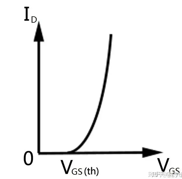
1. Transfer characteristic curve
The transfer characteristic curve describes the relationship between the output collector current IC and the gate-emitter voltage VGE. This characteristic can be compared to the working principle of MOSFET to deepen understanding. When the gate-source voltage VGS is zero, it is equivalent to forming two back-to-back pn junctions between the source S and the drain D, which makes at least one pn junction in the reverse direction no matter how large the drain-source voltage VDS is or what polarity it is Bias state, so that no conduction channel is created, the device cannot be turned on, and the drain-source current ID is very close to zero. When 0<VGS<VGS(th), as the gate voltage increases, an electric field is formed on the lower surface of the gate oxide, attracting a small amount of electrons, but due to the limited number of electrons, an effective conductive channel cannot be formed, and the drain-source current ID remains about zero. When VGS≥VGS(th), the electric field is enhanced, attracting more electrons, making the P region of the substrate invert, forming a conductive channel, thereby reducing the resistance between the drain and source electrodes. At this time, when the drain-source voltage is applied, the MOSFET will enter the conduction state. ID is linear with VGS over most of the drain-source current range.
In IGBT, VGE is similar to VGS in MOSFET, and IC is similar to ID of MOSFET. When VGE≥VGE(th), a conductive channel is formed in the IGBT, making the device turn on.
2. Output characteristic curve
The output characteristic curve describes the relationship between drain-source current IC and collector-emitter voltage VCE under different gate-emitter voltage VGE. Since IGBT can be equivalent to a combination of MOSFET and PNP structure, its output characteristics are closely related to MOSFET. Here still take MOSFET as an example to explain its output characteristics.
When VDS is small and positive, with the increase of VDS, ID increases gradually. In this area, it is called variable resistance area in MOSFET, and it is called non-saturation area in IGBT. As VDS continues to increase, the slope of the ID-VDS curve gradually decreases and approaches zero. In MOSFETs this is called the constant current region and in IGBTs it is called the saturation region. When VDS increases to avalanche breakdown, no matter in MOSFET or IGBT, this region is called breakdown region.
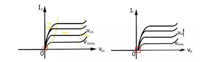
In IGBT, VGE is similar to VGS of MOSFET, IC is similar to ID of MOSFET, and VCE is similar to VDS of MOSFET. Between the linear region and the saturation region, there are some differences between MOSFETs and IGBTs. This is mainly due to the fact that in the initial stage of IGBT conduction, a voltage drop of about 0.7V is required to change the emitter P+/N- junction from zero bias to forward bias.
IGBT Working Principle
An IGBT works by activating or deactivating its gate terminal to achieve an on or off state.
When a positive input voltage is applied to the gate, the drive circuit remains on, turning on the emitter. Conversely, if the IGBT's gate voltage is zero or slightly negative, the circuit will be turned off.
IGBT can have the functions of BJT and MOS tube at the same time, and its gain is reflected in the ratio between the output signal and the control input signal.
In a traditional BJT, the amount of gain (commonly called Beta or β) is roughly the same as the ratio of output current to input current. For MOS tubes, since the gate terminal isolates the main channel from carrying current, there is no input current. The gain of the IGBT is determined by dividing the change in output current by the change in input voltage.
An N-channel IGBT will conduct when the collector is at a positive potential with respect to the emitter. At the same time, the gate is also maintained at a sufficient positive potential (greater than VGET) relative to the emitter, an inversion layer is formed directly under the gate, a channel is formed, and the current flows from the collector to the emitter.

In an IGBT, the collector current Ic consists of two parts Ie and Ih. Ie is the current that injects electrons through the injection layer, drift layer, and finally forms a channel that flows from the collector to the emitter. Ih is the hole current flowing from collector to emitter through Q1 and bulk resistance Rb. Therefore, it can be approximately considered that Ic ≈ Ie.
In the IGBT, there is also a special phenomenon called the "latch-up" phenomenon of the IGBT. This happens when the collector current exceeds a certain threshold (ICE). In this case, the parasitic thyristor is locked, the gate terminal loses control of the collector current, and the IGBT cannot be turned off even if the gate potential drops below VGET. At this time, in order to turn off the IGBT, it is necessary to adopt a typical commutation circuit, such as forced commutation using a thyristor. Failure to turn off the device in a timely manner may result in damage to the device.
Final Words
It is precisely because the insulated gate bipolar transistor (IGBT) combines the advantages of the bipolar transistor (BJT) and the metal oxide semiconductor field effect transistor (MOSFET), it has been widely used in many fields, bringing various applications Huge benefit. Through the above detailed description, readers have a preliminary understanding of the basic principles and characteristics of IGBT, and this knowledge will play an important role in daily applications.
Read More:
Difference Between BJT, MOSFET and IGBT: BJT vs MOSFET vs IGBT
IGCT vs. IGBT: What Are the Difference
IGBT vs GTO: Difference Between IGBT and GTO
IGBT Structure, Characteristics and Working Principle
Application of IGBT and IGBT Application Examples
IGBT Symbol Diagram, Characteristics, Circuit
Global IGBT Shortage: Cause & Future Outlook
IGBT Rectifier: All You Want to Know
IGBT Types: Understanding the Basics
How to Test an IGBT with A Multimeter
Difference Between IGBT and MOSFET (IGBT vs MOSFET)
What is the Advantage of IGBT
Difference Between IGBT and Thyristor
Latest Blogs
Popular Manufacturers